Datasheet 搜索 > AD转换器 > ADI(亚德诺) > AD7788BRMZ-REEL 数据手册 > AD7788BRMZ-REEL 其他数据使用手册 4/8 页
 器件3D模型
¥ 15.126
AD7788BRMZ-REEL 其他数据使用手册 - ADI(亚德诺)
制造商:
ADI(亚德诺)
分类:
AD转换器
封装:
MSOP-10
描述:
低功耗, 16位/ 24位Σ-Δ型ADC Low Power, 16-/24-Bit, Sigma-Delta ADCs
Pictures:
3D模型
符号图
焊盘图
引脚图
产品图
页面导航:
技术参数、封装参数在P4
应用领域在P7P8

导航目录
AD7788BRMZ-REEL数据手册
Page:
of 8 Go
若手册格式错乱,请下载阅览PDF原文件
–4–
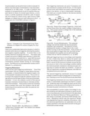
A quick analysis can be performed on site to evaluate if a
device may have been overstressed or may have been
subjected to an ESD event. In order to perform this
analysis, to compare the pin-to-pin I/V results of the sus-
pect device to those of a known good device, a curve
tracer or similar equipment should be used. A typical
set of I/V traces for a short circuit, open circuit or ESD
leakage on a digital input pin (with reference to the V
SS
supply pin) of a 12-bit DAC is shown in Figure 7.
OPEN CIRCUIT
SHORT CIRCUIT
V/DIV. : 2V
I/DIV. : 50A
GOOD TRACE
ESD LEAKAGE
Figure 7. Example of an Unpowered Curve Trace
Analysis of a Digital Pin versus a Supply Pin (V
SS
)
LATCH-UP
Latch-up is a potentially destructive situation in which a
parasitic active device is triggered, shorting the positive
and negative supplies together. If current flow is not
limited, electrical overstress will occur. The classic case
of latch-up occurs in CMOS output devices, in which the
driver transistors and wells form a
pnpn
SCR structure
when one of the two parasitic base-emitter junctions is
momentarily forward biased during an overvoltage
event. The SCR turns on and essentially causes a short
between V
DD
and ground.
Triggering Mechanisms
There are two main triggering mechanisms.
First
, if the
input/output (I/O) pin voltage is raised above the posi-
tive supply, or lowered below the negative supply, one
of the parasitic transistors is turned on. The current re-
turning to the supply through the collector causes a volt-
age drop across the base-emitter of the second parasitic
transistor. In turn, the collector current of the second
transistor maintains a forward bias on the base-emitter
of the first transistor. If the product of the two transistor
gains is greater than unity, the condition may be self-
sustaining and can persist even after the external volt-
age is removed.
OUTPUT
V
DD
R
SUB
GND
RWELL
OUTPUT
QP
QN
Figure 8. Parasitic SCR. The Diffusions in a CMOS
output form a parasitic SCR. The resistors are labeled
for an n-well process.
This triggering mechanism can occur if excessive volt-
age overshoot is present at the I/O pin, or if the signal
arrives at the input before the power supplies are ap-
plied to the device, or due to electrostatic discharge.
This latch-up is usually limited to the devices directly
connected to the pin.
Figure 9a. Output Overvoltage Triggering. Initial hole
current flows when the output voltage is raised above
V
DD
. This current causes a voltage rise in the substrate
under the NMOS device.
Figure 9b. Current Multiplication. The substrate
voltage rise actively biases the second parasitic
transistor into conduction. The electron current
subsequently causes a voltage drop in the n-well,
further turning on the first transistor. If the product of
the current gains is larger than one, the final current
flow between the supplies can be self-sustaining,
limited only by internal resistance’s, i.e., an SCR.
Although triggering is by an overvoltage event (typically
of only a diode drop above or below the power sup-
plies), the industry practice is to classify the I/O suscepti-
bility in terms of the amount of excess current the pin
can source or sink in this overvoltage condition before
the internal parasitic resistance's develop enough volt-
age drop to sustain the latch-up condition. A value of
100 mA is generally considered adequate, with 200 mA
considered immune to latch-up.
The
second
triggering mechanism occurs if a supply
voltage is raised enough to break down an internal junc-
tion, injecting current into the SCR previously described.
This triggering mechanism can occur due to supply tran-
sients, or electrostatic discharges shunted to a supply
rail. Unlike the case of I/O triggering, latch-up can occur
anywhere on the die and is not limited to the vicinity of
the external power connections or I/O pins.
The susceptibility to power supply overvoltage is usu-
ally limited by the fabrication process on which the de-
vice is manufactured, and can be found in the data sheet
under the Absolute Maximum Rating specification. If
this rating is exceeded, permanent EOS damage may
occur. Operating a device near the maximum ratings
may degrade the long term reliability of the device. Also
the electrical specifications are applicable only at the
supply specified on the data sheet and will not be guar-
anteed above these ratings.
p+ n+ n+ p+ p+ n+
n-well
p-sub
GND OUTPUT
OUTPUTGND
V
DD
ε
–
+
V
DD
p+ n+ n+ p+ p+ n+
n-well
p-sub
GND OUTPUT
V
DD
OUTPUT
GND
R
SUB
ε
–
+
INPUT
INPUT
器件 Datasheet 文档搜索
AiEMA 数据库涵盖高达 72,405,303 个元件的数据手册,每天更新 5,000 多个 PDF 文件
