Datasheet 搜索 > AD转换器 > ADI(亚德诺) > AD7788BRMZ-REEL 数据手册 > AD7788BRMZ-REEL 其他数据使用手册 5/8 页
 器件3D模型
¥ 15.134
AD7788BRMZ-REEL 其他数据使用手册 - ADI(亚德诺)
制造商:
ADI(亚德诺)
分类:
AD转换器
封装:
MSOP-10
描述:
低功耗, 16位/ 24位Σ-Δ型ADC Low Power, 16-/24-Bit, Sigma-Delta ADCs
Pictures:
3D模型
符号图
焊盘图
引脚图
产品图
页面导航:
技术参数、封装参数在P4
应用领域在P7P8

导航目录
AD7788BRMZ-REEL数据手册
Page:
of 8 Go
若手册格式错乱,请下载阅览PDF原文件
–5–
Design Rules
The following is a set of rules to be followed for all de-
signers using CMOS and Bipolar-CMOS ICs:
5
1. Digital inputs and outputs should not be allowed to
exceed V
DD
by more than 0.3 volts at any time. This
includes a power-down situation when V
DD
= 0 volts.
2. Digital inputs and outputs should also not be allowed
to go below DGND by more than –0.3 volts.
3. For mixed signal devices, DGND should not be al-
lowed to exceed AGND by 0.3 volts.
4. For a CMOS or Bipolar-CMOS DAC, I
OUT
should, in
general, not be allowed to drop below AGND by more
than 0.3 volts. Some DACs can tolerate significant
I
OUT
current flow, however, without any danger of
latch-up.
Latch-Up Prevention Techniques
The following recommendations should be imple-
mented in general, for all applications with CMOS and
Bipolar-CMOS ICs that violate one or more of the previ-
ously discussed rules:
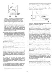
1. If the digital inputs or outputs of a device can go be-
yond V
DD
at any time, a diode (such as a 1N914) con-
nected in series with V
DD
will prevent SCR action and
subsequent latch-up. This works because the diode
prevents the base current of the parasitic lateral-PNP
transistor from flowing out the V
DD
pin, thus prevent-
ing SCR triggering. This is shown in Figure 10.
Diodes are also a reliable solution if power-up se-
quencing is identified as the failure mechanism. In
such a case, the insertion of a Schottky diode be-
tween the logic inputs and the V
DD
supply rail (the
anode of the diode connected to the logic inputs), will
ensure that the logic inputs do not exceed the V
DD
supply by more than 0.3 volts, thus preventing latch-
up of the device.
Ib
≈
0
Ic
=
0
R
p-well
I
DGND
≈
0
DGND
R
SUB
V
DD
IC POWERED UP
IC#1
R
OUT
IC#2
I
DD
≈
0
1N914
0V+5V
IC POWERED DOWN
DGND
COMMON GROUND
OUTPUT
INPUT
I
IN
≈
0
V
DD
Figure 10. Adding an inexpensive silicon diode in
series with the V
DD
pin of the unpowered IC effec-
tively prevents the parasitic lateral-PNP transistor’s
base current from flowing and inhibits SCR action.
However, the one
exception
to this rule is when the
input range of a device exceeds the supply voltage
range of the device, e.g., by design the AD7893-10 12-
bit A/D subsystem, the input range is ±10 V and the
supply is +5 V.
2. If the digital inputs and outputs of a device can go
below DGND at any time, a Schottky diode (such as
an HP5082-2835) connected from those inputs or out-
puts to DGND will effectively clamp negative excur-
sions at –0.3 volts to –0.4 volts. This prevents the
emitter-base junction of the parasitic NPN transistor
from being turned on, and also prevents SCR
triggering. Figure 11 shows the connections for the
Schottky diodes.
R
p-well
DGND
R
SUB
V
DD
IC#1
R
OUT
IC#2
1N914
+5V
DGND
COMMON GROUND
V
DD
R
IN
C
IN
HP5082-
2835
LR
DAMPING
PARASITIC
TRACE
INDUCTANCE
I/P
HP5082-
2835
OUTPUT
+5V
0V
–0.3
INPUT CLAMPED
AND DAMPED
Figure 11. Adding Schottky diodes from the inputs
and outputs of a CMOS IC to DGND protects against
undervoltages causing conduction of the parasitic
NPN, thus inhibiting SCR action. The series damp-
ing resistor makes ringing due to long PC board
traces die out more quickly.
3. If the DGND potential can occasionally exceed AGND
by more than 0.3 volts, a Schottky diode placed be-
tween the two pins of the device will prevent conduc-
tion of the associated parasitic NPN transistor. This
provides additional protection against latch-up as
shown in Figure 12. An extra diode connected in in-
verse parallel with the one just mentioned provides
clamping of DGND to AGND in the other direction
and will help to minimize digital noise from being in-
jected into the IC.
To identify over- and under-voltage events as described
in points (2) and (3) above, the use of a storage oscillo-
scope is suggested, set at the maximum ratings specifi-
cation for each pin. Set the Time/Div. to the minimum
setting on the oscilloscope (preferably in the ns range).
This test should be conducted over a long period of
time, e.g., overnight.
4. In circuits where the I
OUT
pin of a CMOS IC can be
pulled below AGND, another Schottky diode clamp
between these two terminals will prevent sensitive
器件 Datasheet 文档搜索
AiEMA 数据库涵盖高达 72,405,303 个元件的数据手册,每天更新 5,000 多个 PDF 文件
