Datasheet 搜索 > 开发套件 > Integrated Device Technology(艾迪悌) > ADC0808S250-DB 数据手册 > ADC0808S250-DB 其他数据使用手册 1/22 页

¥ 0
ADC0808S250-DB 其他数据使用手册 - Integrated Device Technology(艾迪悌)
制造商:
Integrated Device Technology(艾迪悌)
分类:
开发套件
Pictures:
3D模型
符号图
焊盘图
引脚图
产品图
页面导航:
导航目录
ADC0808S250-DB数据手册
Page:
of 22 Go
若手册格式错乱,请下载阅览PDF原文件

®
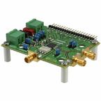
ADC0808S125/250
Single 8-bit ADC, up to 125 MHz or 250 MHz
Rev. 04 — 2 July 2012 Product data sheet
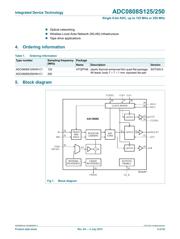
1. General description
The ADC0808S is a differential, high-speed, 8-bit Analog-to-Digital Converter (ADC)
optimized for telecommunication transmission control systems and tape drive
applications. It allows signal sampling frequencies up to 250 MHz.
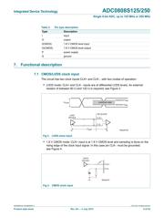
The ADC0808S clock inputs are selectable between 1.8 V Complementary Metal Oxide
Sem
iconductor (CMOS) or Low-Voltage Differential Signals (LVDS). The data output
signal levels are 1.8 V CMOS.
All static digital inputs (CLKSEL, CCSSEL, CE_N,
OTC, DEL0 and DEL1) are 1.8 V
CMOS compatible.
The ADC0808S offers the most flexible acquisition
control system possible due to its
programmable Complete Conversion Signal (CCS) which allows the delay time of the
acquisition clock and acquisition clock frequency to be adjusted.
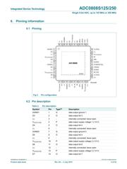
The ADC0808S is supplied in an HTQFP48 package.
2. Features
8-bit resolution
Hig
h-speed sampling rate up to 250 MHz
Ma
ximum analog input frequency up to 560 MHz
Pr
ogrammable acquisition output clock (complete conversion signal)
Dif
ferential analog input
Integ
rated voltage regulator or external control for analog input full-scale
Integ
rated voltage regulator for input common-mode reference
Se
lectable 1.8 V CMOS or LVDS clock input
1.
8 V CMOS digital outputs
1.
8 V CMOS compatible static digital inputs
Bina
ry or 2’s complement CMOS outputs
Only 2 clock cycles latency
Ind
ustrial temperature range from 40 C to +85 C
HTQF
P48 package
3. Applications
2.5G and 3G cellular base infrastructure radio transceivers
Wireless ac
cess systems
Fixed t
elecommunications
器件 Datasheet 文档搜索
AiEMA 数据库涵盖高达 72,405,303 个元件的数据手册,每天更新 5,000 多个 PDF 文件
