Datasheet 搜索 > 开发套件 > Integrated Device Technology(艾迪悌) > ADC0808S250-DB 数据手册 > ADC0808S250-DB 其他数据使用手册 6/22 页

¥ 0
ADC0808S250-DB 其他数据使用手册 - Integrated Device Technology(艾迪悌)
制造商:
Integrated Device Technology(艾迪悌)
分类:
开发套件
Pictures:
3D模型
符号图
焊盘图
引脚图
产品图
页面导航:
导航目录
ADC0808S250-DB数据手册
Page:
of 22 Go
若手册格式错乱,请下载阅览PDF原文件

ADC0808S125_ADC0808S250_4 © IDT 2012. All rights reserved.
Product data sheet Rev. 04 — 2 July 2012 6 of 22
Integrated Device Technology
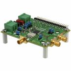
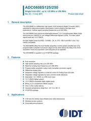
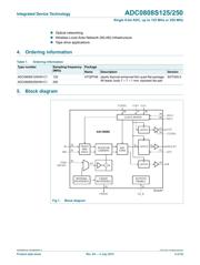
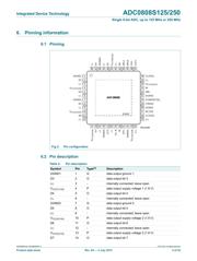
ADC0808S125/250
Single 8-bit ADC, up to 125 MHz or 250 MHz
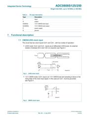
Table 4. Clock input format selection
Pin CLKSEL Clock input signal
Pins CLK+ and CLK
HIGH or not connected LVDS
LOW 1.8 V CMOS
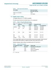
7.2 Digital output coding
The digital outputs are 1.8 V CMOS compatible.
The data output format can be either
binary or 2’s complement.
Table 5. Output coding with differential inputs
V
i(p-p)
= 2.0 V; V
ref(fs)
= 1.25 V; typical values to AGND.
Code Inputs (V) Output Outputs D7 to D0
V
i(IN)
V
i(INN)
Pin IR Binary 2’s complement
Underflow < 0.45 > 1.45 LOW 0000 0000 1000 0000
0 0.45 1.45 HIGH 0000 0000 1000 0000
1 - - HIGH 0000 0001 1000 0001
: : : : : :
127 0.95 0.95 HIGH 0111 1111 1111 1111
: : : : : :
254 - - HIGH 1111 1110 0111 1110
255 1.45 0.45 HIGH 1111 1111 0111 1111
Overflow > 1.45 < 0.45 LOW 1111 1111 0111 1111
The in-range CMOS output pin IR will be HIGH during normal operation. When the ADC
input reaches either positive or negative full-scale, the IR output will be LOW.
Selection between output coding is controlled by pins OTC and CE_N.
Table 6. Output format selection
2’s complement outputs Chip enable Output data
Pin OTC Pin CE_N Pins D0 to D7, CCS and IR
LOW LOW active; binary
HIGH LOW active; 2’s complement
X
[1]
HIGH high-impedance
[1] X = don’t care.
器件 Datasheet 文档搜索
AiEMA 数据库涵盖高达 72,405,303 个元件的数据手册,每天更新 5,000 多个 PDF 文件
