Datasheet 搜索 > 开发套件 > TI(德州仪器) > ADC08D1000DEV/NOPB 数据手册 > ADC08D1000DEV/NOPB 其他数据使用手册 3/40 页


¥ 35212.309
ADC08D1000DEV/NOPB 其他数据使用手册 - TI(德州仪器)
制造商:
TI(德州仪器)
分类:
开发套件
Pictures:
3D模型
符号图
焊盘图
引脚图
产品图
ADC08D1000DEV/NOPB数据手册
Page:
of 40 Go
若手册格式错乱,请下载阅览PDF原文件
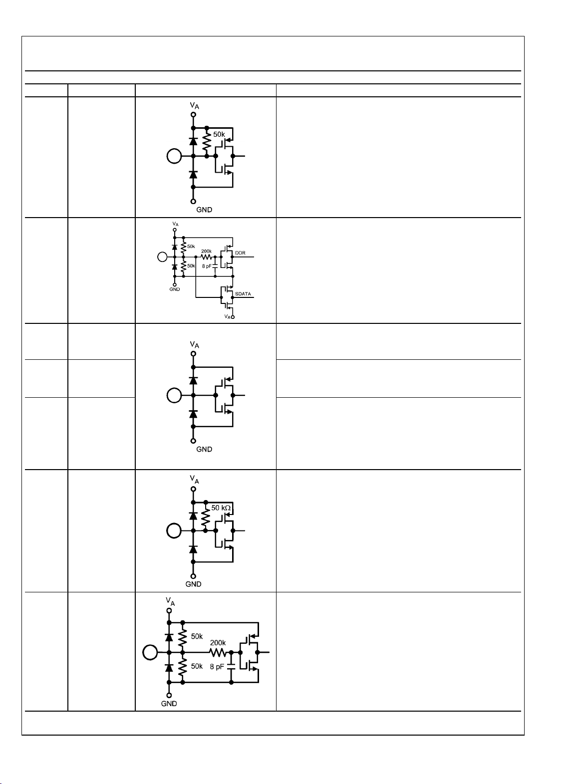
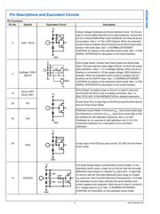
Pin Descriptions and Equivalent Circuits
Pin Functions
Pin No. Symbol Equivalent Circuit Description
3 OutV / SCLK
Output Voltage Amplitude and Serial Interface Clock. Tie this pin
high for normal differential DCLK and data amplitude. Ground this
pin for a reduced differential output amplitude and reduced power
consumption. See1.1.6 The LVDS Outputs. When the extended
control mode is enabled, this pin functions as the SCLK input which
clocks in the serial data. See 1.2 NORMAL/EXTENDED
CONTROL for details on the extended control mode. See 1.3 THE
SERIAL INTERFACE for description of the serial interface.
4
OutEdge / DDR /
SDATA
DCLK Edge Select, Double Data Rate Enable and Serial Data
Input. This input sets the output edge of DCLK+ at which the output
data transitions. (See 1.1.5.2 OutEdge Setting). When this pin is
floating or connected to 1/2 the supply voltage, DDR clocking is
enabled. When the extended control mode is enabled, this pin
functions as the SDATA input. See 1.2 NORMAL/EXTENDED
CONTROL for details on the extended control mode. See 1.3 THE
SERIAL INTERFACE for description of the serial interface.
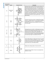
15
DCLK_RST/
DCLK_RST-
DCLK Reset. A positive pulse on this pin is used to reset and
synchronize the DCLK outs of multiple converters. See 1.5
MULTIPLE ADC SYNCHRONIZATION for detailed description.
26
PD
Power Down Pins. A logic high on the PD pin puts the entire device
into the Power Down Mode.
30 CAL
Calibration Cycle Initiate. A minimum t
CAL_L
input clock cycles logic
low followed by a minimum of t
CAL_H
input clock cycles high on this
pin initiates the self calibration sequence. See 2.4.2 Self
Calibration for an overview of self-calibration and 2.4.2.2 On-
Command Calibration for a description of on-command
calibration.
29
PDQ
A logic high on the PDQ pin puts only the "Q" ADC into the Power
Down mode.
14 FSR/ECE
Full Scale Range Select and Extended Control Enable. In non-
extended control mode, a logic low on this pin sets the full-scale
differential input range to a reduced V
IN
input level . A logic high
on this pin sets the full-scale differential input range to a higher
V
IN
input level. See Converter Electrical Characteristics. To enable
the extended control mode, whereby the serial interface and
control registers are employed, allow this pin to float or connect it
to a voltage equal to V
A
/2. See 1.2 NORMAL/EXTENDED
CONTROL for information on the extended control mode.
3 www.national.com
ADC08D1000
器件 Datasheet 文档搜索
AiEMA 数据库涵盖高达 72,405,303 个元件的数据手册,每天更新 5,000 多个 PDF 文件
