Datasheet 搜索 > 开发套件 > TI(德州仪器) > ADC08D1000DEV/NOPB 数据手册 > ADC08D1000DEV/NOPB 其他数据使用手册 4/40 页


¥ 35179.501
ADC08D1000DEV/NOPB 其他数据使用手册 - TI(德州仪器)
制造商:
TI(德州仪器)
分类:
开发套件
Pictures:
3D模型
符号图
焊盘图
引脚图
产品图
ADC08D1000DEV/NOPB数据手册
Page:
of 40 Go
若手册格式错乱,请下载阅览PDF原文件
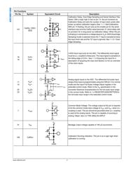
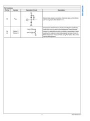
Pin Functions
Pin No. Symbol Equivalent Circuit Description
127
CalDly / DES /
SCS
Calibration Delay, Dual Edge Sampling and Serial Interface Chip
Select. With a logic high or low on pin 14, this pin functions as
Calibration Delay and sets the number of input clock cycles after
power up before calibration begins (See 1.1.1 Self-Calibration).
With pin 14 floating, this pin acts as the enable pin for the serial
interface input and the CalDly value becomes "0" (short delay with
no provision for a long power-up calibration delay). When this pin
is floating or connected to a voltage equal to V
A
/2, DES (Dual Edge
Sampling) mode is selected where the "I" input is sampled at twice
the input clock rate and the "Q" input is ignored. See 1.1.5.1 Dual-
Edge Sampling.
18
19
CLK+
CLK-
LVDS Clock input pins for the ADC. The differential clock signal
must be a.c. coupled to these pins. The input signal is sampled on
the falling edge of CLK+. See 1.1.2 Acquiring the Input for a
description of acquiring the input and Section 2.3 for an overview
of the clock inputs.
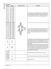
11
10
22
23
V
IN
I+
V
IN
I−
V
IN
Q+
V
IN
Q−
Analog signal inputs to the ADC. The differential full-scale input
range of this input is programmable using the FSR pin 14 in normal
mode and the Input Full-Scale Voltage Adjust register in the
extended control mode. Refer to the V
IN
specification in the
Converter Electrical Characteristics for the full-scale input range
in the normal mode. Refer to 1.4 REGISTER DESCRIPTION for
the full-scale input range in the extended control mode.
7
V
CMO
Common Mode Voltage. The voltage output at this pin is required
to be the common mode input voltage at V
IN
+ and V
IN
− when d.c.
coupling is used. This pin should be grounded when a.c. coupling
is used at the analog inputs. This pin is capable of sourcing or
sinking 100μA. See 2.2 THE ANALOG INPUT.
31
V
BG
Bandgap output voltage capable of 100 μA source/sink.
126 CalRun
Calibration Running indication. This pin is at a logic high when
calibration is running.
www.national.com 4
ADC08D1000
器件 Datasheet 文档搜索
AiEMA 数据库涵盖高达 72,405,303 个元件的数据手册,每天更新 5,000 多个 PDF 文件
