Datasheet 搜索 > ADI(亚德诺) > ADN4668 数据手册 > ADN4668 其他数据使用手册 1/6 页

¥ 0
ADN4668 其他数据使用手册 - ADI(亚德诺)
制造商:
ADI(亚德诺)
描述:
3 V LVDS四通道CMOS差分线路接收器 3 V LVDS Quad CMOS Differential Line Receiver
Pictures:
3D模型
符号图
焊盘图
引脚图
产品图
页面导航:
技术参数、封装参数在P1
导航目录
ADN4668数据手册
Page:
of 6 Go
若手册格式错乱,请下载阅览PDF原文件

AN-1179
APPLICATION NOTE
One Technology Way • P. O. Box 9106 • Norwood, MA 02062-9106, U.S.A. • Tel: 781.329.4700 • Fax: 781.461.3113 • www.analog.com
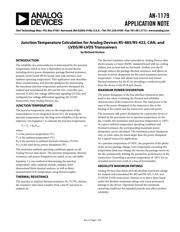
Junction Temperature Calculation for Analog Devices RS-485/RS-422, CAN, and
LVDS/M-LVDS Transceivers
by Richard Anslow
INTRODUCTION
The reliability of a semiconductor is determined by the junction
temperature, which in turn is dependent on several factors
including device power dissipation, package thermal resistance,
printed circuit board (PCB) layout, heat sink interface, and
ambient operating temperature. This application note describes
these considerations, and provides guidance for determining
the maximum junction temperature and power dissipated for
isolated and nonisolated RS-485 and RS-422, controller area
network (CAN), low voltage differential signaling (LVDS), and
multipoint low voltage differential signaling (M-LVDS)
transceivers from Analog Devices, Inc.
JUNCTION TEMPERATURE
The junction temperature refers to the temperature of the
semiconductor in an integrated circuit (IC). By keeping the
junction temperature low, the long-term reliability of the device
improves. Use Equation 1 to estimate the junction temperature.
T
J
= T
A
+ θ
JA
P
DISS
(1)
where:
T
J
is the junction temperature (°C).
T
A
is the ambient temperature (°C).
θ
JA
is the junction to ambient thermal resistance (°C/W).
P
DISS
is the total device power dissipation (W).
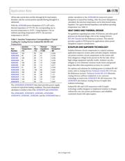
The maximum ambient operating conditions appear on all
Analog Devices data sheets. The junction temperature, thermal
resistance, and power dissipation are stated, or are calculable.
Equation 1 is one method of determining the junction
temperature; other methods include complex, three-
dimensional finite element analyses, as well as direct
measurement of IC temperature using thermocouples.
THERMAL RESISTANCE
The junction to ambient thermal resistance, θ
JA
(°C/W), defines
the resistance when heat transfers from a hot IC junction to
ambient air.
The thermal resistance values provided in Analog Devices data
sheets assume a 4-layer JEDEC standard board with no cooling
airflow, and no heat sink on the board. Airflow over the IC
package reduces the package thermal resistance, and allows an
increase in power dissipation for the rated maximum junction
temperature. A heat sink allows heat removal and a lower
thermal resistance for the IC by providing a conduction path
from the device to the PCB and chassis.
MAXIMUM POWER DISSIPATION
The power dissipation of the bus interface (transceiver plus
load) is key when evaluating the thermal and reliability
characteristics of the transceiver device. The total power is the
sum of the power dissipated in the transceiver due to the
loading of the output and the transceiver quiescent power.
The maximum safe power dissipation for a particular device is
limited by the associated rise in junction temperature on the
die. Usually, the maximum rated junction temperature is 150°C.
At a given ambient temperature operating condition and
thermal resistance, the corresponding maximum power
dissipation can be calculated. The maximum power dissipation
may, in some cases, be much larger than the power dissipated
for a typical transceiver application.
At a junction temperature of 150°C, the properties of the plastic
of the device package change. Even temporarily exceeding this
temperature limit may change the stresses the package exerts on
the die, permanently shifting the parametric performance of the
transceivers. Exceeding a junction temperature of 150°C for an
extended period may result in a loss of functionality.
ABSOLUTE MAXIMUM RATINGS
Analog Devices data sheets provide absolute maximum ratings
for isolated and nonisolated RS-485 and RS-422, CAN, and
LVDS/M-LVDS transceivers. Stresses at or above those listed
under the absolute maximum ratings may cause permanent
damage to the device. Operation beyond the maximum
operating conditions for extended periods may affect product
reliability.
Rev. A | Page 1 of 6
器件 Datasheet 文档搜索
AiEMA 数据库涵盖高达 72,405,303 个元件的数据手册,每天更新 5,000 多个 PDF 文件

