Datasheet 搜索 > ADI(亚德诺) > ADN4668 数据手册 > ADN4668 其他数据使用手册 4/6 页


¥ 0
ADN4668 其他数据使用手册 - ADI(亚德诺)
制造商:
ADI(亚德诺)
描述:
3 V LVDS四通道CMOS差分线路接收器 3 V LVDS Quad CMOS Differential Line Receiver
Pictures:
3D模型
符号图
焊盘图
引脚图
产品图
页面导航:
技术参数、封装参数在P1
导航目录
ADN4668数据手册
Page:
of 6 Go
若手册格式错乱,请下载阅览PDF原文件

AN-1179 Application Note
Rev. A | Page 4 of 6
M-LVDS TRANSCEIVERS
Analog Devices M-LVDS transceivers expand on the
established LVDS signaling method by allowing bidirectional
communication between more than two nodes. The
ADN4690E, ADN4692E, ADN4694E, and ADN4695E are
transceivers for transmitting and receiving M-LVDS at high
speeds (data rates of up to 100 Mbps). The ADN4691E,
ADN4693E, ADN4696E, and ADN4697E are capable of
operating at data rates of up to 200 Mbps. The M-LVDS
transceivers are available in full and half-duplex modes, with
8-lead and 14-lead SOIC packages. The AN-1177 Application Note
provides an LVDS and M-LVDS circuit implementation guide.
The ADN4690E/ADN4692E/ADN4694E/ADN4695E data
sheet provides information for calculating the power dissipated
and junction temperature, depending on the package type.
Table 3 provides the thermal impedance values for 8-lead and
14-lead SOIC packages.
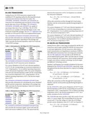
Table 3. Information for 100 Mbps M-LVDS Transceivers
M-LVDS Part
Number
T
A
Max
(°C)
Thermal
Impedance
(°C/W)
SOIC
Package
Type Duplex
ADN4690E 85 121 8-lead Half
ADN4694E 85 121 8-lead Half
ADN4692E 85 86 14-lead Full
ADN4695E 85 86 14-lead Full
The ADN4690E/ADN4692E/ADN4694E/ADN4695E data
sheet specifies 94 mW transceiver power dissipation.
For a power dissipation of 94 mW and a thermal impedance
of 121°C/W, the corresponding rise in junction temperature is
11°C. Using Equation 1 for an ambient operating temperature
of 85°C, the junction temperature is 96°C. For a power dissipation
of 94 mW and a thermal impedance of 86°C/W, the corresponding
rise in junction temperature is 8°C. Using Equation 1 for an
ambient operating temperature of 85°C, the junction temper-
ature is 93°C.
The ADN4691E/ADN4693E/ADN4696E/ADN4697E data
sheet provides information for calculating the power dissipated
and the junction temperature, depending on the package type.
Table 4 provides the thermal impedance values for 8-lead and
14-lead SOIC packages.
Table 4. Information for 200 Mbps M-LVDS Transceivers
M-LVDS Part
Number
T
A
Max
(°C)
Thermal
Impedance
(°C/W)
SOIC
Package
Type Duplex
ADN4691E 85 121 8-lead Half
ADN4696E 85 121 8-lead Half
ADN4693E 85 86 14-lead Full
ADN4697E 85 86 14-lead Full
The ADN4691E/ADN4693E/ADN4696E/ADN4697E data
sheet provides the maximum supply current with both the
driver and receiver enabled at 25 mA. The typical load (R
L
)
driven by the transceiver is 50 Ω. Use Equation 4 to calculate
the total power dissipated.
P
DISS
= VI − I
2
R
L
= (3.3 V)(25 mA) − (10 mA)
2
(50 )
= 77 mW (4)
All bus side current does not flow through the R
L
load resistor;
therefore, only the current portion typically flowing through R
L
is
subtracted.
For a power dissipation of 77 mW and a thermal impedance of
121°C/W, the corresponding rise in junction temperature is
9°C. Using Equation 1 for an ambient operating temperature of
85°C, the junction temperature is 94°C.
For a power dissipation of 77 mW and a thermal impedance of
86°C/W, the corresponding rise in junction temperature is 7°C.
Using Equation 1 for an ambient operating temperature of
85°C, the junction temperature is 92°C.
RS-485/RS-422 TRANSCEIVERS
Analog Devices offers a wide range of standard RS-485/RS-422
transceivers and iCoupler isolated RS-485/RS-422 transceivers
to suit many applications. RS-485 transceivers allow bidirec-
tional communication over long distances (maximum of 4000 ft),
with differential transmission lines increasing noise immunity.
The AN-960 Application Note provides an RS-485/RS-422
circuit implementation guide. Table 5 provides data for Analog
Devices isolated RS-485 transceivers, which include integrated
iCoupler and isoPower isolation technology (see the iCoupler
and isoPower Technology section).
Equation 5 and Equation 6 are example calculations for the power
dissipated in the ADM2587E and ADM2582E, respectively, using
data gathered from the device data sheet for a typical 54 loading
condition.
P
DISS
= VI − I
2
R
L
= (5 V)(98 mA) + (3.3 V)(35 mA) −
(27 mA)
2
(54 ) = 567 mW (5)
P
DISS
= VI − I
2
R
L
= (5 V)(200 mA) + (3.3 V)(50 mA) −
(27 mA)
2
(54 ) = 1.13 W (6)
All bus side current does not flow through the R
L
load resistor;
therefore, only the current portion typically flowing through R
L
is
subtracted.
For the ADM2587E, with a power dissipation of 0.567 W and a
thermal impedance of 50°C/W, the corresponding rise in junction
temperature is 28°C. Using Equation 1 for an ambient operating
temperature of 85°C, the junction temperature is 113°C. Use a
similar calculation for the ADM2582E.
The ADM2486 data sheet specifies a logic side current of 4 mA
with a 5 V power supply. The corresponding 58 mA bus side
current and 5 V bus side voltage (at a data rate of 20 Mbps)
provide a power dissipation value of 271 mW (see Equation 7).
P
DISS
= VI − I
2
R
L
= (5 V)(4 mA) + (5 V)(58 mA) −
(27 mA)
2
(54 ) = 271 mW (7)
器件 Datasheet 文档搜索
AiEMA 数据库涵盖高达 72,405,303 个元件的数据手册,每天更新 5,000 多个 PDF 文件
