Datasheet 搜索 > ADI(亚德诺) > ADN4668 数据手册 > ADN4668 其他数据使用手册 3/6 页


¥ 0
ADN4668 其他数据使用手册 - ADI(亚德诺)
制造商:
ADI(亚德诺)
描述:
3 V LVDS四通道CMOS差分线路接收器 3 V LVDS Quad CMOS Differential Line Receiver
Pictures:
3D模型
符号图
焊盘图
引脚图
产品图
页面导航:
技术参数、封装参数在P1
导航目录
ADN4668数据手册
Page:
of 6 Go
若手册格式错乱,请下载阅览PDF原文件
Application Note AN-1179
Rev. A | Page 3 of 6
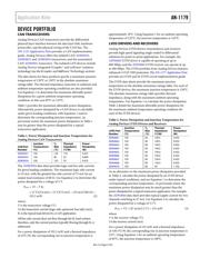
DEVICE PORTFOLIO
CAN TRANSCEIVERS
Analog Devices CAN transceivers provide the differential
physical layer interface between the data layer link, hardware
protocoller, and the physical wiring of the CAN bus. The
AN-1123 Application Note provides a CAN implementation
guide. Analog Devices offers the isolated CAN ADM3052,
ADM3053, and ADM3054 transceivers, and the nonisolated
CAN ADM3051 transceiver. The isolated CAN devices include
Analog Devices integrated iCoupler ® and isoPower® isolation
technology (see the iCoupler and isoPower Technology section).
The data sheets for these products specify a maximum junction
temperature of 130°C or 150°C in the absolute maximum
ratings table. The thermal impedance (junction to ambient) and
ambient temperature operating conditions are also provided.
Use Equation 1 to determine the maximum allowable power
dissipation for a given ambient temperature operating
condition, in this case 85°C or 125°C.
Table 1 provides the maximum allowable power dissipation.
Alternatively, power dissipated by a CAN device is calculable
under given loading conditions, with Equation 1 used to
determine the corresponding junction temperature. As
previously noted, the maximum power dissipation in Table 1
may be greater than the power dissipated for a typical
transceiver application.
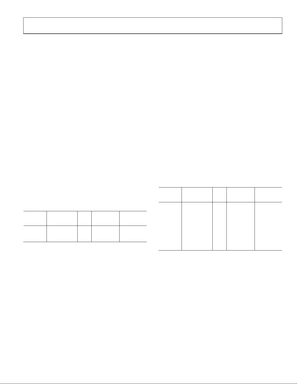
Table 1. Power Dissipation and Junction Temperature for
Analog Devices CAN Transceivers
CAN Part
Number
Junction
Temperature
(°C)
T
A
Max
(°C)
Thermal
Impedance
(°C/W)
Power
Dissipation
(W)
ADM3051 150 125 110 0.227
ADM3053 130 85 53 0.849
ADM3054 150 125 53 0.472
The ADM3054 data sheet provides logic and bus side currents
for given loading conditions. The maximum logic side current
is 3.0 mA, with the greatest bus side current of 75 mA for an
output load resistance of 60 Ω. Use Equation 2 to determine the
power dissipated for a voltage of 5 V.
P
DISS
= VI − I
2
R
L
= (5 V)(3.0 mA) + (5 V)(75 mA) − (25 mA)
2
(60 ) =
352.5 mW (2)
where:
V is the transceiver voltage (V).
I is the transceiver current (logic side, quiescent, bus side) (mA).
R
L
is the typical load driven by a CAN application.
All bus side current does not flow through the R
L
load resistor;
therefore, only the current portion typically flowing through R
L
is
subtracted.
For a power dissipation of 352.5 mW and a thermal impedance
of 53°C/W, the corresponding rise in junction temperature is
approximately 18°C. Using Equation 1 for an ambient operating
temperature of 125°C, the junction temperature is 143°C.
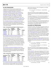
LVDS DRIVERS AND RECEIVERS
Analog Devices LVDS drivers (transmitters) and receivers
provide high speed signaling single-ended to differential
solutions for point-to-point applications. For example, the
ADN4663 LVDS driver is capable of operating at up to
600 Mbps, and the ADN4664 LVDS receiver can operate at up
to 400 Mbps. The LVDS portfolio from Analog Devices features
enhanced ±15 kV ESD protection. The AN-1177 Application Note
provides an LVDS and M-LVDS circuit implementation guide.
The LVDS data sheets provide the maximum junction
temperature in the absolute maximum ratings table. For each of
the LVDS devices, the maximum junction temperature is 150°C.
The absolute maximum ratings table specifies thermal
impedance, along with the maximum ambient operating
temperature. Use Equation 1 to calculate the power dissipation.
Table 2 details the maximum allowable power dissipation for
the maximum ambient temperature operating condition for
each of the LVDS devices.
Table 2. Power Dissipation and Junction Temperature for
Analog Devices LVDS Drivers and Receivers
LVDS Part
Number
Junction
Temperature
(°C)
T
A
Max
(°C)
Thermal
Impedance
(°C/W)
Power
Dissipation
(W)
ADN4661 150 85 149.5 0.435
ADN4662 150 85 149.5 0.435
ADN4663 150 85 149.5 0.435
ADN4664 150 85 149.5 0.435
ADN4665 150 85 150.4 0.432
ADN4666 150 85 150.4 0.432
ADN4667 150 85 150.4 0.432
ADN4668 150 85 150.4 0.432
ADN4670 150 85 59 1.102
As an alternative to the maximum power dissipation provided
in Table 2, calculate the power dissipated by an LVDS device
under typical conditions, and use Equation 1 to determine the
corresponding junction temperature. As previously noted, the
maximum power dissipation may be much greater than the
power dissipated for a typical transceiver application. For example,
the ADN4664 data sheet provides typical supply current for two
channels switching at 47 mA. Use Equation 3 to calculate the
power dissipated for a voltage of 3.3 V.
P
DISS
= VI = (47 mA)(3.3 V) = 155 mW (3)
where:
V is the receiver voltage (V).
I is the receiver current (mA).
For a power dissipation of 155 mW and a thermal impedance
of 149.5°C/W, the corresponding rise in junction temperature is
23°C. Using Equation 1 for an ambient operating temperature
of 85°C, the junction temperature is 108°C.
器件 Datasheet 文档搜索
AiEMA 数据库涵盖高达 72,405,303 个元件的数据手册,每天更新 5,000 多个 PDF 文件
