Datasheet 搜索 > MOS管 > TI(德州仪器) > CSD25481F4 数据手册 > CSD25481F4 其他数据使用手册 4/26 页

¥ 0.381
CSD25481F4 其他数据使用手册 - TI(德州仪器)
制造商:
TI(德州仪器)
分类:
MOS管
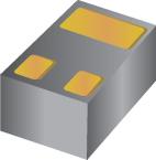
封装:
PICOSTAR-3
描述:
P 通道 NexFET 功率 MOSFET,CSD25481W4
Pictures:
3D模型
符号图
焊盘图
引脚图
产品图
页面导航:
导航目录
CSD25481F4数据手册
Page:
of 26 Go
若手册格式错乱,请下载阅览PDF原文件
CSD87381P
ZHCSAY2F –MARCH 2013–REVISED MARCH 2015
www.ti.com.cn
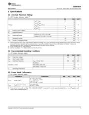
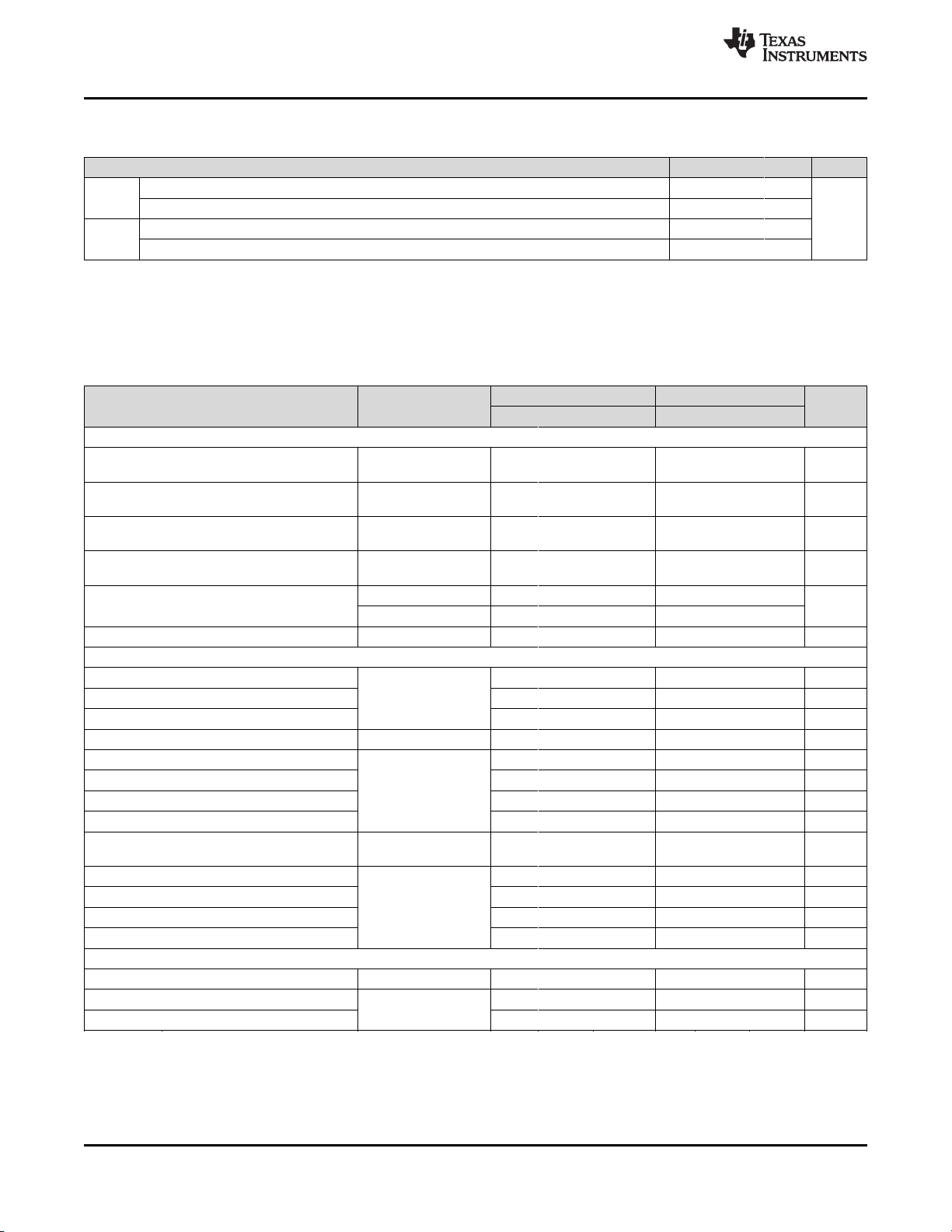
5.4 Thermal Information
T
A
= 25°C (unless otherwise stated)
THERMAL METRIC MIN TYP MAX UNIT
Junction-to-ambient thermal resistance (min Cu)
(1)
184
R
θJA
Junction-to-ambient thermal resistance (max Cu)
(2)(1)
84
°C/W
Junction-to-case thermal resistance (top of package)
(1)
4.9
R
θJC
Junction-to-case thermal resistance (P
GND
pin)
(1)
1.65
(1) R
θJC
is determined with the device mounted on a 1 inch
2
(6.45 cm
2
), 2 oz. (0.071 mm thick) Cu pad on a 1.5 inches × 1.5 inches
(3.81 cm × 3.81 cm), 0.06 inch (1.52 mm) thick FR4 board. R
θJC
is specified by design while R
θJA
is determined by the user’s board
design.
(2) Device mounted on FR4 material with 1 inch
2
(6.45 cm
2
) Cu.
5.5 Electrical Characteristics
T
A
= 25°C (unless otherwise stated)
Q1 Control FET Q2 Sync FET
PARAMETER TEST CONDITIONS UNIT
MIN TYP MAX MIN TYP MAX
STATIC CHARACTERISTICS
Drain-to-Source Voltage V
GS
= 0 V, I
DS
= 250 30 30 V
BV
DSS
μA
Drain-to-Source Leakage Current V
GS
= 0 V, V
DS
= 24
I
DSS
1 1 μA
V
Gate-to-Source Leakage Current V
DS
= 0 V, V
GS
= 10
I
GSS
100 100 nA
V
Gate-to-Source Threshold V
DS
= V
GS
, I
DS
= 250
V
GS(th)
1.1 1.9 1 1.7 V
Voltage μA
V
GS
= 4.5 V, I
DS
= 8 A 15.7 18.9 7 8.4
R
DS(on)
Drain-to-Source On-Resistance mΩ
V
GS
= 8 V, I
DS
= 8 A 13.6 16.3 6.3 7.6
g
ƒs
Transconductance V
DS
= 10 V, I
DS
= 8 A 40 89 S
DYNAMIC CHARACTERISTICS
C
ISS
Input Capacitance
(1)
434 564 1020 1320 pF
V
GS
= 0 V, V
DS
= 15
C
OSS
Output Capacitance
(1)
V, 225 293 308 400 pF
ƒ = 1 MHz
C
RSS
Reverse Transfer Capacitance
(1)
9.1 11.8 40 52 pF
R
G
Series Gate Resistance
(1)
5 6.4 1.25 2.5 Ω
Q
g
Gate Charge Total (4.5 V)
(1)
3.9 5 8.9 11.5 nC
Q
gd
Gate Charge – Gate-to-Drain 0.9 2.5 nC
V
DS
= 15 V,
I
DS
= 8 A
Q
gs
Gate Charge – Gate-to-Source 1.2 2 nC
Q
g(th)
Gate Charge at V
th
0.7 1.3 nC
Output Charge V
DD
= 12 V, V
GS
= 0 4.9 8.5 nC
Q
OSS
V
t
d(on)
Turn On Delay Time 6.7 7.9 ns
V
DS
= 15 V, V
GS
= 4.5
t
r
Rise Time 19.3 16.3 ns
V,
t
d(off)
Turn Off Delay Time 10.6 16.8 ns
I
DS
= 8 A, R
G
= 2 Ω
t
ƒ
Fall Time 3 2.9 ns
DIODE CHARACTERISTICS
V
SD
Diode Forward Voltage I
DS
= 8 A, V
GS
= 0 V 0.85 0.79 V
Q
rr
Reverse Recovery Charge 8 16 nC
V
dd
= 15 V, I
F
= 8 A,
di/dt = 300 A/μs
t
rr
Reverse Recovery Time 13 17 ns
(1) Specified by design
4 Copyright © 2013–2015, Texas Instruments Incorporated
器件 Datasheet 文档搜索
AiEMA 数据库涵盖高达 72,405,303 个元件的数据手册,每天更新 5,000 多个 PDF 文件
