Datasheet 搜索 > MOS管 > TI(德州仪器) > CSD87355Q5D 数据手册 > CSD87355Q5D 其他数据使用手册 3/23 页


¥ 16.774
CSD87355Q5D 其他数据使用手册 - TI(德州仪器)
制造商:
TI(德州仪器)
分类:
MOS管
封装:
LSON-CLIP
描述:
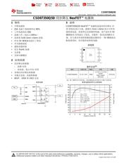
CSD87355Q5D 同步降压 NexFET™ 电源块
Pictures:
3D模型
符号图
焊盘图
引脚图
产品图
页面导航:
导航目录
CSD87355Q5D数据手册
Page:
of 23 Go
若手册格式错乱,请下载阅览PDF原文件
3
CSD87350Q5D
www.ti.com.cn
ZHCS110E –MARCH 2011–REVISED FEBRUARY 2017
Copyright © 2011–2017, Texas Instruments Incorporated
(1) Stresses beyond those listed under Absolute Maximum Ratings may cause permanent damage to the device. These are stress ratings
only, and functional operation of the device at these or any other conditions beyond those indicated in the Recommended Operating
Conditions is not implied. Exposure to absolute-maximum-rated conditions for extended periods may affect device reliability.
(2) Pulse duration ≤ 50 µs. Duty cycle ≤ 0.01%.
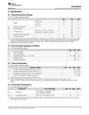
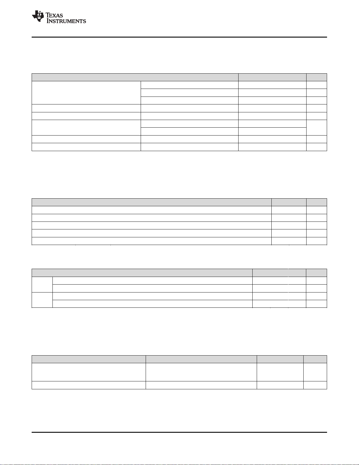
5 Specifications
5.1 Absolute Maximum Ratings
T
A
= 25°C (unless otherwise noted)
(1)
MIN MAX UNIT
Voltage
V
IN
to P
GND
–0.8 30 V
T
G
to T
GR
–8 10 V
B
G
to P
GND
–8 10 V
I
DM
Pulsed current rating
(2)
120 A
P
D
Power dissipation 12 W
E
AS
Avalanche energy
Sync FET, I
D
= 105 A, L = 0.1 mH 551
mJ
Control FET, I
D
= 60 A, L = 0.1 mH 180
T
J
Operating junction temperature –55 150 °C
T
stg
Storage temperature –55 150 °C
5.2 Recommended Operating Conditions
T
A
= 25° (unless otherwise noted)
MIN MAX UNIT
V
GS
Gate drive voltage 4.5 8 V
V
IN
Input supply voltage 27 V
ƒ
SW
Switching frequency C
BST
= 0.1 μF (min) 200 1500 kHz
Operating current 40 A
T
J
Operating temperature 125 °C
(1) Device mounted on FR4 material with 1-in
2
(6.45-cm
2
) Cu.
(2) R
θJC
is determined with the device mounted on a 1-in
2
(6.45-cm
2
), 2-oz (0.071-mm) thick Cu pad on a 1.5-in × 1.5-in
(3.81-cm × 3.81-cm), 0.06-in (1.52-mm) thick FR4 board. R
θJC
is specified by design while R
θJA
is determined by the user’s board
design.
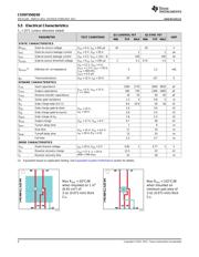
5.3 Thermal Information
T
A
= 25°C (unless otherwise stated)
THERMAL METRIC MIN TYP MAX UNIT
R
θJA
Junction-to-ambient thermal resistance (min Cu)
(1)(2)
102 °C/W
Junction-to-ambient thermal resistance (max Cu)
(1)(2)
50 °C/W
R
θJC
Junction-to-case thermal resistance (top of package)
(2)
20 °C/W
Junction-to-case thermal resistance (P
GND
pin)
(2)
2 °C/W
(1) Measurement made with six 10-µF (TDK C3216X5R1C106KT or equivalent) ceramic capacitors placed across V
IN
to P
GND
pins and
using a high-current 5-V driver IC.
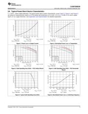
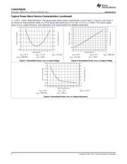
5.4 Power Block Performance
T
A
= 25° (unless otherwise noted)
PARAMETER TEST CONDITIONS MIN TYP MAX UNIT
P
LOSS
Power loss
(1)
V
IN
= 12 V V
GS
= 5 V, V
OUT
= 1.3 V,
I
OUT
= 25 A, ƒ
SW
= 500 kHz,
L
OUT
= 0.3 µH, T
J
= 25°C
3 W
I
QVIN
V
IN
quiescent current T
G
to T
GR
= 0 V ,B
G
to P
GND
= 0 V 10 µA
器件 Datasheet 文档搜索
AiEMA 数据库涵盖高达 72,405,303 个元件的数据手册,每天更新 5,000 多个 PDF 文件
