Datasheet 搜索 > 地磁传感器 > TI(德州仪器) > DRV5023BIQLPGMQ1 数据手册 > DRV5023BIQLPGMQ1 其他数据使用手册 4/34 页

¥ 5.947
DRV5023BIQLPGMQ1 其他数据使用手册 - TI(德州仪器)
制造商:
TI(德州仪器)
分类:
地磁传感器
封装:
TO-92-3
描述:
汽车类 2.7V 至 38V 霍尔效应单极开关 3-TO-92 -40 to 125
Pictures:
3D模型
符号图
焊盘图
引脚图
产品图
页面导航:
引脚图在P3P4Hot
典型应用电路图在P22P23
原理图在P9
封装尺寸在P27P29P30
焊盘布局在P25
标记信息在P27
封装信息在P27P28P29P30
技术参数、封装参数在P4
电气规格在P5P6
导航目录
DRV5023BIQLPGMQ1数据手册
Page:
of 34 Go
若手册格式错乱,请下载阅览PDF原文件

4
DRV8846
ZHCSG92A –JUNE 2014–REVISED MARCH 2017
www.ti.com.cn
Copyright © 2014–2017, Texas Instruments Incorporated
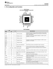
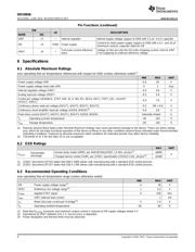
Pin Functions (continued)
PIN
I/O DESCRIPTION
NAME NO.
VINT 17 — Internal regulator Internal supply voltage; bypass to GND with 2.2-μF, 6.3-V capacitor
VM 15 PWR Power supply
Connect to motor power supply; bypass to GND with a 0.1- and 10-μF
(minimum) ceramic capacitor rated for VM
VREF 14 I
Full-scale current reference
input
Voltage on this pin sets the full scale chopping current; short to VINT
if not supplying an external reference voltage
(1) Stresses beyond those listed under Absolute Maximum Ratings may cause permanent damage to the device. These are stress ratings
only, which do not imply functional operation of the device at these or any other conditions beyond those indicated under Recommended
Operating Conditions. Exposure to absolute-maximum-rated conditions for extended periods may affect device reliability.
(2) Transients of ±1 V for less than 25 ns are acceptable.
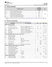
6 Specifications
6.1 Absolute Maximum Ratings
over operating free-air temperature referenced with respect to GND (unless otherwise noted)
(1)
MIN MAX UNIT
Power supply voltage (VM) –0.3 20 V
Power supply voltage ramp rate (VM) 0 2 V/µs
Internal regulator voltage (VINT) –0.3 3.6 V
Analog input pin voltage (VREF) –0.3 3.6 V
Control pin voltage (nENABLE, STEP, DIR, I0, I1, M0, M1, DEC0, DEC1, TOFF_SEL, nSLEEP,
nFAULT, ADEC)
–0.3 7.0 V
Continuous phase node pin voltage (AOUT1, AOUT2, BOUT1, BOUT2) –0.3 VM + 0.6 V
Continuous shunt amplifier input pin voltage (AISEN, BISEN)
(2)
–0.6 0.6 V
Peak drive current (AOUT1, AOUT2, BOUT1, BOUT2, AISEN, BISEN) Internally limited A
T
J
Operating junction temperature –40 150 °C
T
stg
Storage temperature –65 150 °C
(1) JEDEC document JEP155 states that 500-V HBM allows safe manufacturing with a standard ESD control process.
(2) JEDEC document JEP157 states that 250-V CDM allows safe manufacturing with a standard ESD control process.
6.2 ESD Ratings
MAX UNIT
V
(ESD)
Electrostatic
discharge
Human body model (HBM), per ANSI/ESDA/JEDEC JS-001, all pins
(1)
±4000
V
Charged device model (CDM), per JEDEC specification JESD22-C101, all pins
(2)
±1500
(1) Note that R
DS(ON)
increases and maximum output current is reduced at VM supply voltages below 5 V
(2) Operational at VREF between 0 to 1 V, but accuracy is degraded
(3) Power dissipation and thermal limits must be observed
6.3 Recommended Operating Conditions
over operating free-air temperature range (unless otherwise noted)
MIN MAX UNIT
VM Power supply voltage range
(1)
4 18 V
VREF Reference rms voltage range
(2)
1 3.3 V
ƒ
PWM
Applied STEP signal 0 250 kHz
I
VINT
VINT external load current 1 mA
I
FS
Motor full-scale current per H-bridge
(3)
0 1.4 A
T
A
Operating ambient temperature –40 85 °C
器件 Datasheet 文档搜索
AiEMA 数据库涵盖高达 72,405,303 个元件的数据手册,每天更新 5,000 多个 PDF 文件
