Datasheet 搜索 > 电机驱动器 > TI(德州仪器) > DRV8833PW 数据手册 > DRV8833PW 其他数据使用手册 4/33 页
 器件3D模型
¥ 21.162
DRV8833PW 其他数据使用手册 - TI(德州仪器)
制造商:
TI(德州仪器)
分类:
电机驱动器
封装:
TSSOP-16
描述:
具有电流调节功能的 10.8V、2A、双路 H 桥电机驱动器 16-TSSOP -40 to 85
Pictures:
3D模型
符号图
焊盘图
引脚图
产品图
页面导航:
导航目录
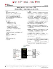
DRV8833PW数据手册
Page:
of 33 Go
若手册格式错乱,请下载阅览PDF原文件
4
DRV8302
ZHCS138C –AUGUST 2011–REVISED MARCH 2016
www.ti.com.cn
Copyright © 2011–2016, Texas Instruments Incorporated
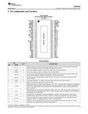
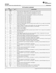
Pin Functions (continued)
PIN
I/O
(1)
DESCRIPTION
NO. NAME
13 GVDD P Internal gate driver voltage regulator. GVDD cap should connect to GND
14 CP1 P Charge pump pin 1, ceramic cap should be used between CP1 and CP2
15 CP2 P Charge pump pin 2, ceramic cap should be used between CP1 and CP2
16 EN_GATE I Enable gate driver and current shunt amplifiers. Control buck via EN_BUCK pin.
17 INH_A I PWM Input signal (high side), half-bridge A
18 INL_A I PWM Input signal (low side), half-bridge A
19 INH_B I PWM Input signal (high side), half-bridge B
20 INL_B I PWM Input signal (low side), half-bridge B
21 INH_C I PWM Input signal (high side), half-bridge C
22 INL_C I PWM Input signal (low side), half-bridge C
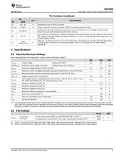
23 DVDD P
Internal 3.3-V supply voltage. DVDD cap should connect to AGND. This is an output, but not specified
to drive external circuitry.
24 REF I
Reference voltage to set output of shunt amplfiiers with a bias voltage which equals to half of the
voltage set on this pin. Connect to ADC reference in microcontroller.
25 SO1 O Output of current amplifier 1
26 SO2 O Output of current amplifier 2
27 AVDD P
Internal 6-V supply voltage, AVDD cap should connect to AGND. This is an output, but not specified to
drive external circuitry.
28 AGND P Analog ground pin
29 PVDD1 P
Power supply pin for gate driver and current shunt amplifier. PVDD1 is independent of buck power
supply, PVDD2. PVDD1 cap should connect to GND
30 SP2 I
Input of current amplifier 2 (connecting to positive input of amplifier). Recommend to connect to ground
side of the sense resistor for the best commom mode rejection.
31 SN2 I Input of current amplifier 2 (connecting to negative input of amplifier).
32 SP1 I
Input of current amplifier 1 (connecting to positive input of amplifier). Recommend to connect to ground
side of the sense resistor for the best commom mode rejection.
33 SN1 I Input of current amplifier 1 (connecting to negative input of amplifier).
34 SL_C I
Low-Side MOSFET source connection, half-bridge C. Low-side V
DS
measured between this pin and
SH_C.
35 GL_C O Gate drive output for Low-Side MOSFET, half-bridge C
36 SH_C I
High-Side MOSFET source connection, half-bridge C. High-side V
DS
measured between this pin and
PVDD1.
37 GH_C O Gate drive output for High-Side MOSFET, half-bridge C
38 BST_C P Bootstrap cap pin for half-bridge C
39 SL_B I
Low-Side MOSFET source connection, half-bridge B. Low-side V
DS
measured between this pin and
SH_B.
40 GL_B O Gate drive output for Low-Side MOSFET, half-bridge B
41 SH_B I
High-Side MOSFET source connection, half-bridge B. High-side V
DS
measured between this pin and
PVDD1.
42 GH_B O Gate drive output for High-Side MOSFET, half-bridge B
43 BST_B P Bootstrap cap pin for half-bridge B
44 SL_A I
Low-Side MOSFET source connection, half-bridge A. Low-side V
DS
measured between this pin and
SH_A.
45 GL_A O Gate drive output for Low-Side MOSFET, half-bridge A
46 SH_A I
High-Side MOSFET source connection, half-bridge A. High-side V
DS
measured between this pin and
PVDD1.
47 GH_A O Gate drive output for High-Side MOSFET, half-bridge A
48 BST_A P Bootstrap cap pin for half-bridge A
49 BIAS I Bias pin. Connect 1M-Ω resistor to GND, or 0.1 µF capacitor to GND.
50, 51 PH O The source of the internal high side MOSFET of buck converter
器件 Datasheet 文档搜索
AiEMA 数据库涵盖高达 72,405,303 个元件的数据手册,每天更新 5,000 多个 PDF 文件
