Datasheet 搜索 > 电机驱动器 > TI(德州仪器) > DRV8833PW 数据手册 > DRV8833PW 其他数据使用手册 5/33 页
 器件3D模型
¥ 21.162
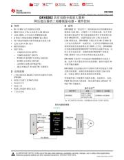
DRV8833PW 其他数据使用手册 - TI(德州仪器)
制造商:
TI(德州仪器)
分类:
电机驱动器
封装:
TSSOP-16
描述:
具有电流调节功能的 10.8V、2A、双路 H 桥电机驱动器 16-TSSOP -40 to 85
Pictures:
3D模型
符号图
焊盘图
引脚图
产品图
页面导航:
导航目录
DRV8833PW数据手册
Page:
of 33 Go
若手册格式错乱,请下载阅览PDF原文件
5
DRV8302
www.ti.com.cn
ZHCS138C –AUGUST 2011–REVISED MARCH 2016
Copyright © 2011–2016, Texas Instruments Incorporated
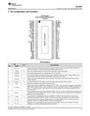
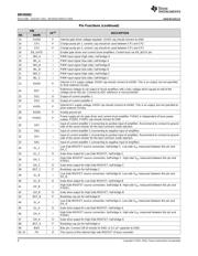
Pin Functions (continued)
PIN
I/O
(1)
DESCRIPTION
NO. NAME
52 BST_BK P Bootstrap cap pin for buck converter
53, 54 PVDD2 P Power supply pin for buck converter, PVDD2 cap should connect to GND.
55 EN_BUCK I
Enable buck converter. Internal pullup current source. Pull below 1.2 V to disable. Float to enable.
Adjust the input undervoltage lockout with two resistors
56 SS_TR I
Buck soft-start and tracking. An external capacitor connected to this pin sets the output rise time. Since
the voltage on this pin overrides the internal reference, it can be used for tracking and sequencing. Cap
should connect to GND
57
GND
(PWR_PAD)
P
GND pin. The exposed power pad must be electrically connected to ground plane through soldering to
PCB for proper operation and connected to bottom side of PCB through vias for better thermal
spreading.
(1) Stresses beyond those listed under Absolute Maximum Ratings may cause permanent damage to the device. These are stress ratings
only, which do not imply functional operation of the device at these or any other conditions beyond those indicated under Recommended
Operating Conditions. Exposure to absolute-maximum-rated conditions for extended periods may affect device reliability.
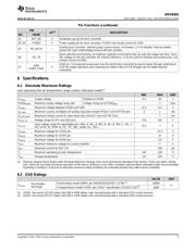
6 Specifications
6.1 Absolute Maximum Ratings
over operating free-air temperature range (unless otherwise noted)
(1)
MIN MAX UNIT
V
PVDD
Supply voltage Relative to PGND –0.3 65 V
PVDD
RAMP
Maximum supply voltage ramp rate Voltage rising up to PVDD
MAX
1 V/µs
V
PGND
Maximum voltage between PGND and GND –0.3 0.3 V
I
IN_MAX
Maximum current, all digital and analog input pins except nFAULT and nOCTW pins –1 1 mA
I
IN_OD_MAX
Maximum sinking current for open-drain pins (nFAULT and nOCTW Pins) 7 mA
V
OPA_IN
Voltage range for SPx and SNx pins –0.6 0.6 V
V
LOGIC
Input voltage range for logic/digital pins (INH_A, INL_A, INH_B, INL_B, INH_C, INL_C,
EN_GATE, M_PWM, M_OC, OC_ADJ, GAIN, DC_CAL)
–0.3 7 V
V
GVDD
Maximum voltage for GVDD pin 13.2 V
V
AVDD
Maximum voltage for AVDD pin 8 V
V
DVDD
Maximum voltage for DVDD pin 3.6 V
V
REF
Maximum reference voltage for current amplifier 7 V
I
REF
Maximum current for REF Pin 100 µA
T
J
Maximum operating junction temperature –40 150 °C
T
stg
Storage temperature –55 150 °C
(1) JEDEC document JEP155 states that 500-V HBM allows safe manufacturing with a standard ESD control process.
(2) JEDEC document JEP157 states that 250-V CDM allows safe manufacturing with a standard ESD control process.
6.2 ESD Ratings
VALUE UNIT
V
(ESD)
Electrostatic
discharge
Human-body model (HBM), per ANSI/ESDA/JEDEC JS-001
(1)
±2000
V
Charged-device model (CDM), per JEDEC specification JESD22-C101
(2)
±500
器件 Datasheet 文档搜索
AiEMA 数据库涵盖高达 72,405,303 个元件的数据手册,每天更新 5,000 多个 PDF 文件
