Datasheet 搜索 > 接口芯片 > TI(德州仪器) > DS36954M 数据手册 > DS36954M 其他数据使用手册 5/9 页
 器件3D模型
¥ 87.552
DS36954M 其他数据使用手册 - TI(德州仪器)
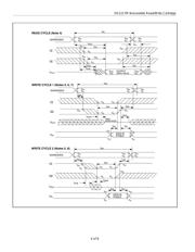
制造商:
TI(德州仪器)
分类:
接口芯片
封装:
SOIC-20
Pictures:
3D模型
符号图
焊盘图
引脚图
产品图
DS36954M数据手册
Page:
of 9 Go
若手册格式错乱,请下载阅览PDF原文件
DS1217M Nonvolatile Read/Write Cartridge
5 of 8
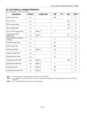
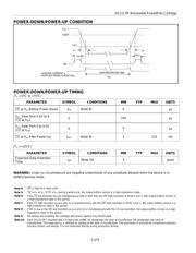
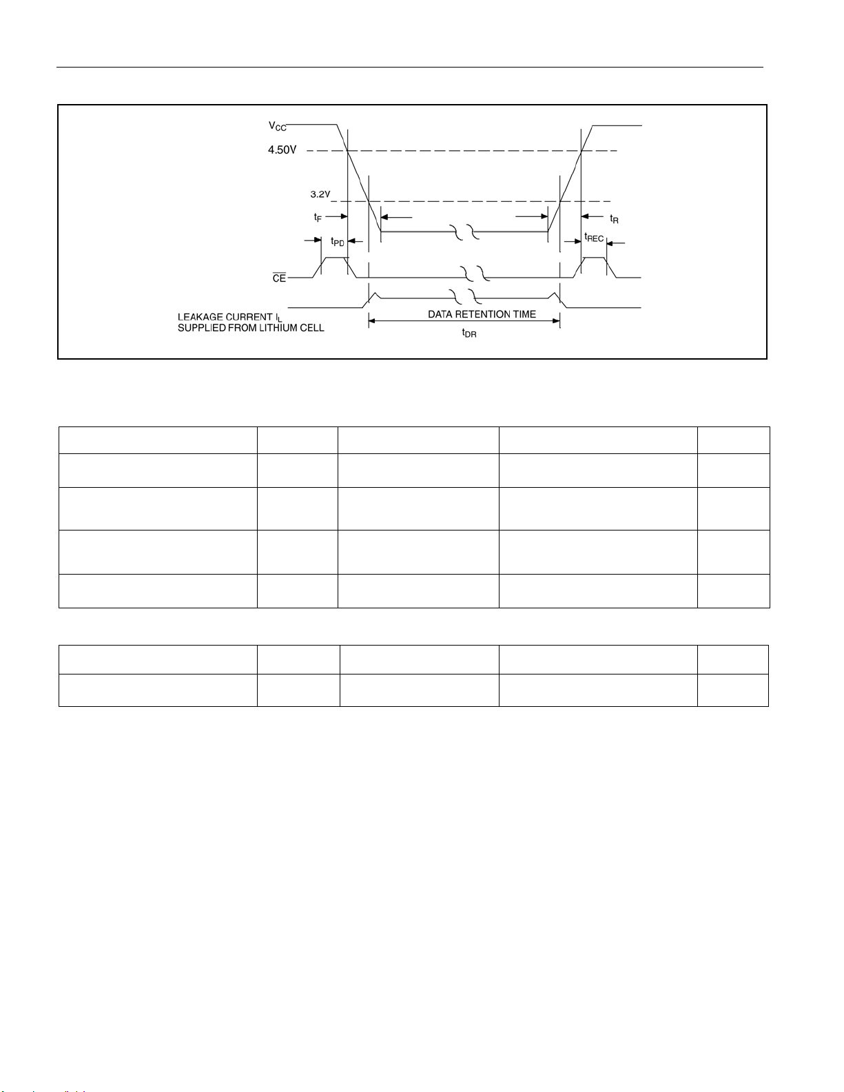
POWER-DOWN/POWER-UP CONDITION
POWER-DOWN/POWER-UP TIMING
(T
A
= 0°C to +70°C)
PARAMETER SYMBOL CONDITIONS MIN TYP MAX UNITS
CE at V
IH
Before Power-Down
t
PD
(Note 9) 0
s
V
CC
Slew from 4.5V to 0
(CE at V
IH
)
t
F
100
s
V
CC
Slew from 0 to 4.5V
(CE at V
IH
)
t
R
0
s
CE at V
IH
After Power-Up
t
REC
(Note 9) 2 125 ms
(T
A
= +25°C)
PARAMETER SYMBOL CONDITIONS MIN TYP MAX UNITS
Expected Data Retention
Time
t
DR
(Note 10) 5 years
WARNING: Under no circumstances are negative undershoots of any amplitude allowed when the device is in
battery-backup mode.
Note 4:
WE is high for a read cycle.
Note 5:
OE = V
IH
or V
IL
. If OE = V
IH
during a write cycle, the output buffers remain in a high-impedance state.
Note 6:
If the CE low transition occurs simultaneously with or later than the WE high transition in Write Cycle 1, that output buffers remain in
a high-impedance state in this period.
Note 7:
If the CE high transition occurs prior to or simultaneously with the WE high transition in Write Cycle 1, the output buffers remain in a
high-impedance state in this period.
Note 8:
If WE is low or the WE low transition occurs prior to or simultaneously with the CE low transition, the output buffers remain in a high-
impedance state in this period.
Note 9: Removing and installing the cartridge with power applied may disturb data.
Note 10: Each DS1217M I smarked with a 4-digit code AABB. AA designates the year of manufacture. BB designates the week of
manufacture. The expected t
DR
is defined as starting at the date of manufacture. This parameter is assured by component selection,
process control, and design. It is not measured directly during production testing.
器件 Datasheet 文档搜索
AiEMA 数据库涵盖高达 72,405,303 个元件的数据手册,每天更新 5,000 多个 PDF 文件
