Datasheet 搜索 > 接口芯片 > TI(德州仪器) > DS36954M 数据手册 > DS36954M 其他数据使用手册 6/9 页
 器件3D模型
¥ 87.544
DS36954M 其他数据使用手册 - TI(德州仪器)
制造商:
TI(德州仪器)
分类:
接口芯片
封装:
SOIC-20
Pictures:
3D模型
符号图
焊盘图
引脚图
产品图
DS36954M数据手册
Page:
of 9 Go
若手册格式错乱,请下载阅览PDF原文件

DS1217M Nonvolatile Read/Write Cartridge
6 of 8
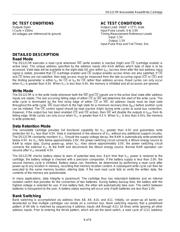
DC TEST CONDITIONS AC TEST CONDITIONS
Outputs Open Output Load: 100pF + 1TTL Gate
t Cycle = 250ns Input Pulse Levels: 0 to 3.0V
All voltages a
re referenced to ground. Timing Measurement Reference Levels
Input: 1.5V
Output: 1.5V
Input Pulse Rise and Fall Times: 5ns
DETAILED DESCRIPTION
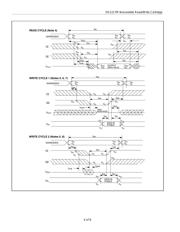
Read Mode
The DS1217M executes a read cycle whenever WE (write enable) is inactive (high) and CE (cartridge enable) is
active (low). The unique address specified by the address inputs (A0–A14) defines which byte of data is to be
accessed. Valid data will be available to the eight data I/O pins within t
ACC
(access time) after the last address input
signal is stable, provided that CE (cartridge enable) and OE (output enable) access times are also satisfied. If OE
and CE times are not satisfied, then data access must be measured from the late occurring signal (CE or OE) and
the limiting parameter is either t
CO
for CE or t
OE
for OE rather than address access. Read cycles can only occur
when V
CC
is greater than 4.5V. When V
CC
is less than 4.5V, the memory is inhibited and all accesses are ignored.
Write Mode
The DS1217M is in the write mode whenever both the WE and CE signals are in the active (low) state after address
inputs are stable. The last occurring falling edge of either CE or WE will determine the start of the write cycle. The
write cycle is terminated by the first rising edge of either CE or WE. All address inputs must be kept valid
throughout the write cycle. WE must return to the high state for a minimum recovery time (t
WR
) before another cycle
can be initiated. The OE control signal should be kept inactive (high) during write cycles to avoid bus contention.
However, if the output bus has been enabled (CE and OE active), then WE will disable the outputs in t
ODW
from its
falling edge. Write cycles can only occur when V
CC
is greater than 4.5 V. When V
CC
is less than 4.5Vs, the memory
is write-protected.
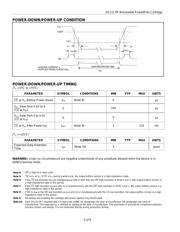
Data Retention Mode
The nonvolatile cartridge provides full functional capability for V
CC
greater than 4.5V and guarantees write
protection for V
CC
less than 4.5V. Data is maintained in the absence of V
CC
without any additional support circuitry.
The DS1217M constantly monitors V
CC
. Should the supply voltage decay, the RAM is automatically write-protected
below 4.5V. As V
CC
falls below approximately 3.0V, the power switching circuit connects a lithium energy source to
RAM to retain data. During power-up, when V
CC
rises above approximately 3.0V, the power switching circuit
connects the external V
CC
to the RAM and disconnects the lithium energy source. Normal RAM operation can
resume after V
CC
exceeds 4.5V.
The DS1217M checks battery status to warn of potential data loss. Each time that V
CC
power is restored to the
cartridge, the battery voltage is checked with a precision comparator. If the battery supply is less than 2.0V, the
second memory cycle is inhibited. Battery status can, therefore, be determined by performing a read cycle after
power-up to any location in memory, recording that memory location content. A subsequent write cycle can then be
executed to the same memory location, altering data. If the next read cycle fails to verify the written data, the
contents of the memory are questionable.
In many applications, data integrity is paramount. The cartridge thus has redundant batteries and an internal
isolation switch that provides for the connection of two batteries. During battery backup time, the battery with the
highest voltage is selected for use. If one battery fails, the other will automatically take over. The switch between
batteries is transparent to the user. A battery status warning will occur only if both batteries are less than 2.0V.
Bank Switching
Bank switching is accomplished via address lines A8, A9, A10, and A11. Initially, on power-up all banks are
deselected so that multiple cartridges can reside on a common bus. Bank switching requires that a predefined
pattern of 64 bits is matched by sequencing 4 address inputs (A8 through A11) 16 times while ignoring all other
address inputs. Prior to entering the 64-bit pattern, which will set the band switch, a read cycle of 1111 (address
器件 Datasheet 文档搜索
AiEMA 数据库涵盖高达 72,405,303 个元件的数据手册,每天更新 5,000 多个 PDF 文件
