Datasheet 搜索 > LVDS、M-LVDS、ECL、CML > TI(德州仪器) > DS90C031W-QMLV 数据手册 > DS90C031W-QMLV 其他数据使用手册 3/11 页

¥ 1853.785
DS90C031W-QMLV 其他数据使用手册 - TI(德州仪器)
制造商:
TI(德州仪器)
分类:
LVDS、M-LVDS、ECL、CML
封装:
DFP
描述:
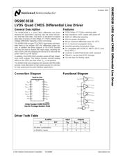
DS90C031QML LVDS四通道CMOS差分线路驱动器 DS90C031QML LVDS Quad CMOS Differential Line Driver
Pictures:
3D模型
符号图
焊盘图
引脚图
产品图
页面导航:
导航目录
DS90C031W-QMLV数据手册
Page:
of 11 Go
若手册格式错乱,请下载阅览PDF原文件
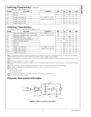
Switching Characteristics (Continued)
V
CC
= +5.0V, T
A
= +25˚C (Notes 3, 6, 9)
Symbol Parameter Conditions Min Typ Max Units
t
TLH
Rise Time 0.35 1.5 ns
t
THL
Fall Time 0.35 1.5 ns
t
PHZ
Disable Time High to Z R
L
= 100Ω,C
L
=5pF
(
Figure 4
and
Figure 5
)
2.5 10 ns
t
PLZ
Disable Time Low to Z 2.5 10 ns
t
PZH
Enable Time Z to High 2.5 10 ns
t
PZL
Enable Time Z to Low 2.5 10 ns
Switching Characteristics
V
CC
= +5.0V
±
10%, T
A
= −40˚C to +85˚C (Notes 3, 6, 9)
Symbol Parameter Conditions Min Typ Max Units
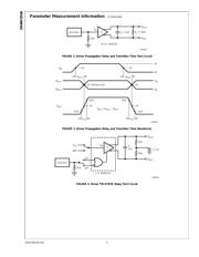
t
PHLD
Differential Propagation Delay High to Low R
L
= 100Ω,C
L
=5pF
(
Figure 2
and
Figure 3
)
0.5 2.0 3.5 ns
t
PLHD
Differential Propagation Delay Low to High 0.5 2.1 3.5 ns
t
SKD
Differential Skew |t
PHLD
–t
PLHD
| 0 80 900 ps
t
SK1
Channel-to-Channel Skew (Note 4) 0 0.3 1.0 ns
t
SK2
Chip to Chip Skew (Note 5) 3.0 ns
t
TLH
Rise Time 0.35 2.0 ns
t
THL
Fall Time 0.35 2.0 ns
t
PHZ
Disable Time High to Z R
L
= 100Ω,C
L
=5pF
(
Figure 4
and
Figure 5
)
2.5 15 ns
t
PLZ
Disable Time Low to Z 2.5 15 ns
t
PZH
Enable Time Z to High 2.5 15 ns
t
PZL
Enable Time Z to Low 2.5 15 ns
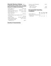
Note 1: “Absolute Maximum Ratings” are those values beyond which the safety of the device cannot be guaranteed. They are not meant to imply that the devices
should be operated at these limits. The table of “Electrical Characteristics” specifies conditions of device operation.
Note 2: Current into device pins is defined as positive. Current out of device pins is defined as negative. All voltages are referenced to ground except: V
OD1
and
∆V
OD1
.
Note 3: All typicals are given for: V
CC
= +5.0V, T
A
= +25˚C.
Note 4: Channel-to-Channel Skew is defined as the difference between the propagation delay of the channel and the other channels in the same chip with an event
on the inputs.
Note 5: Chip to Chip Skew is defined as the difference between the minimum and maximum specified differential propagation delays.
Note 6: Generator waveform for all tests unless otherwise specified:f=1MHz, Z
O
=50Ω,t
r
≤6 ns, and t
f
≤ 6 ns.
Note 7: ESD Ratings:
HBM (1.5 kΩ, 100 pF) ≥ 2kV
EIAJ (0Ω, 200 pF) ≥ 250V
Note 8: Output short circuit current (I
OS
) is specified as magnitude only, minus sign indicates direction only.
Note 9: C
L
includes probe and jig capacitance.
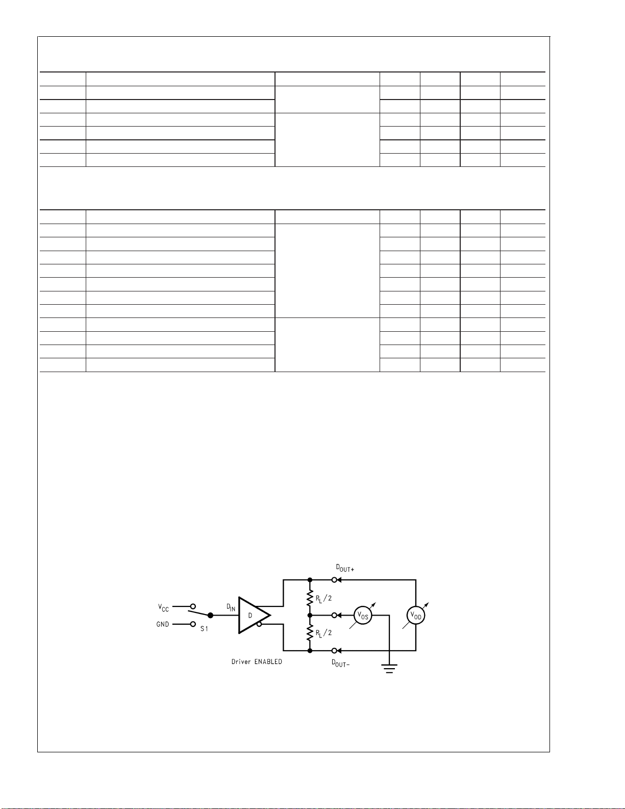
Parameter Measurement Information
10098903
FIGURE 1. Driver V
OD
and V
OS
Test Circuit
DS90C031B
www.national.com3
器件 Datasheet 文档搜索
AiEMA 数据库涵盖高达 72,405,303 个元件的数据手册,每天更新 5,000 多个 PDF 文件
