Datasheet 搜索 > MOS管 > Fairchild(飞兆/仙童) > FDMS6681Z 数据手册 > FDMS6681Z 其他数据使用手册 3/10 页


¥ 11.128
FDMS6681Z 其他数据使用手册 - Fairchild(飞兆/仙童)
制造商:
Fairchild(飞兆/仙童)
分类:
MOS管
封装:
Power-56-8
描述:
FAIRCHILD SEMICONDUCTOR FDMS6681Z 晶体管, MOSFET, P沟道, -49 A, -30 V, 0.0027 ohm, -10 V, -1.7 V
Pictures:
3D模型
符号图
焊盘图
引脚图
产品图
页面导航:


导航目录
FDMS6681Z数据手册
Page:
of 10 Go
若手册格式错乱,请下载阅览PDF原文件
FDMS6681Z P-Channel PowerTrench
®
MOSFET
www.fairchildsemi.com
2©2009 Fairchild Semiconductor Corporation
FDMS6681Z Rev.1.4
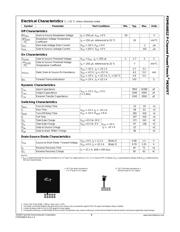
Electrical Characteristics T
J
= 25 °C unless otherwise noted.
Off Characteristics
On Characteristics
Dynamic Characteristics
Switching Characteristics
Drain-Source Diode Characteristics
NOTES:
1. R
θJA
is determined with the device mounted on a 1 in
2
pad 2 oz copper pad on a 1.5 x 1.5 in. board of FR-4 material. R
θJC
is guaranteed by design while R
θCA
is determined by
the user's board design.
2. Pulse Test: Pulse Width < 300 μs, Duty cycle < 2.0%.
3. The diode connected between the gate and source serves only as protection against ESD. No gate overvoltage rating is implied.
4. Pulsed Id please refer to Fig 12 SOA graph for more details.
5. Computed continuous current limited to Max Junction Temperature only, actual continuous current will be limited by thermal electro-mechanical application board design.
Symbol Parameter Test Conditions Min. Typ. Max. Units
BV
DSS
Drain to Source Breakdown Voltage I
D
= -250 μA, V
GS
= 0 V -30 V
ΔBV
DSS
ΔT
J
Breakdown Voltage Temperature
Coefficient
I
D
= -250 μA, referenced to 25 °C 20 mV/°C
I
DSS
Zero Gate Voltage Drain Current V
DS
= -24 V, V
GS
= 0 V -1 μA
I
GSS
Gate to Source Leakage Current V
GS
= ±25 V, V
DS
= 0 V ±10 μA
V
GS(th)
Gate to Source Threshold Voltage V
GS
= V
DS
, I
D
= -250 μA-1-1.7-3V
ΔV
GS(th)
ΔT
J
Gate to Source Threshold Voltage
Temperature Coefficient
I
D
= -250 μA, referenced to 25 °C -7 mV/°C
r
DS(on)
Static Drain to Source On Resistance
V
GS
= -10 V, I
D
= -22.1 A 2.7 3.2
mΩV
GS
= -4.5 V, I
D
= -15.7 A 4.0 5.0
V
GS
= -10 V, I
D
= -22.1 A, T
J
= 125 °C 3.9 5.0
g
FS
Forward Transconductance V
DD
= -10 V, I
D
= -22.1 A 143 S
C
iss
Input Capacitance
V
DS
= -15 V, V
GS
= 0 V,
f = 1 MHz
7803 10380 pF
C
oss
Output Capacitance 1540 2050 pF
C
rss
Reverse Transfer Capacitance 1345 2020 pF
t
d(on)
Turn-On Delay Time
V
DD
= -15 V, I
D
= -22.1 A,
V
GS
= -10 V, R
GEN
= 6 Ω
15 24 ns
t
r
Rise Time 38 61 ns
t
d(off)
Turn-Off Delay Time 260 416 ns
t
f
Fall Time 197 316 ns
Q
g
Total Gate Charge V
GS
= 0 V to -10 V
V
DD
= -15 V,
I
D
= -22.1 A
172 241 nC
Q
g
Total Gate Charge V
GS
= 0 V to -5 V 97 136 nC
Q
gs
Gate to Source Charge 22 nC
Q
gd
Gate to Drain “Miller” Charge 46 nC
V
SD
Source to Drain Diode Forward Voltage
V
GS
= 0 V, I
S
= -2.1 A (Note 2) 0.68 1.2 V
V
GS
= 0 V, I
S
= -22.1 A (Note 2) 0.79 1.25 V
t
rr
Reverse Recovery Time
I
F
= -22.1 A, di/dt = 100 A/μs
44 71 ns
Q
rr
Reverse Recovery Charge 39 63 nC
b. 125 °C/W when mounted on a
minimum pad of 2 oz copper.
a. 50 °C/W when mounted on
a 1 in
2
pad of 2 oz copper.
器件 Datasheet 文档搜索
AiEMA 数据库涵盖高达 72,405,303 个元件的数据手册,每天更新 5,000 多个 PDF 文件
