Datasheet 搜索 > 运算放大器 > TI(德州仪器) > LM7171BIMX/NOPB 数据手册 > LM7171BIMX/NOPB 其他数据使用手册 5/49 页

 器件3D模型
¥ 22.389
LM7171BIMX/NOPB 其他数据使用手册 - TI(德州仪器)
制造商:
TI(德州仪器)
分类:
运算放大器
封装:
SOIC-8
描述:
运算放大器, 高速, 1个放大器, 220 MHz, 4100 V/µs, 5.5V 至 36V, SOIC, 8 引脚
Pictures:
3D模型
符号图
焊盘图
引脚图
产品图
页面导航:
引脚图在P3P4P5Hot
典型应用电路图在P25P26
原理图在P12P25
封装尺寸在P41P43P44P45
焊盘布局在P46
标记信息在P41
封装信息在P41P42P43P44
技术参数、封装参数在P6
应用领域在P30
电气规格在P6P7P8P9
导航目录
LM7171BIMX/NOPB数据手册
Page:
of 49 Go
若手册格式错乱,请下载阅览PDF原文件
5
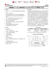
LM5046
www.ti.com.cn
ZHCS581H –FEBRUARY 2011–REVISED NOVEMBER 2014
Copyright © 2011–2014, Texas Instruments Incorporated
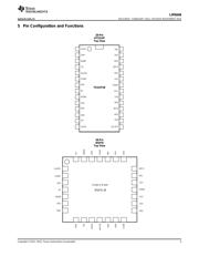
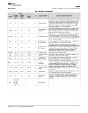
Pin Functions (continued)
PIN
I/O DESCRIPTION APPLICATION INFORMATION
NAME
38 PIN
TSSOP
NO.
28 PIN
TSSOP
NO.
WQFN
NO.
SS 17 13 9 I Soft-Start Input
An internal 20 µA current source charges the SS pin during
start-up. The input to the PWM comparator gradually rises
as the SS capacitor charges to steadily increase the PWM
duty cycle. Pulling the SS pin to a voltage below 200 mV
stops PWM pulses at HO1,2 and LO1,2 and turns off the
synchronous rectifier FETs to a low state.
SSSR 18 14 10 I
Secondary Side
Soft-Start
An external capacitor and an internal 20 µA current source
set the soft-start ramp for the synchronous rectifiers. The
SSSR capacitor charge-up is enabled after the first output
pulse and SS > 2 V and Icomp < 800 µA
SSOFF 19 15 11 I Soft-Stop Disable
When SS OFF pin is connected to the AGND, the LM5046
soft-stops in the event of a VIN UVLO and Hiccup mode
current limit condition. If the SSOFF pin is connected to REF
pin, the controller hard-stops on any fault condition. Refer to
Table 1 for more details.
SR2 25 19 15 O
Synchronous
Rectifier Driver
Control output for synchronous rectifier gate. Capable of
peak sourcing 100 mA and sinking 400 mA.
VCC 27 21 17 I
Output of Start-
Up Regulator
The output voltage of the start-up regulator is initially
regulated to 9.5V. Once the secondary side soft-start (SSSR
pin) reaches 1 V, the VCC output is reduced to 7.7 V. If an
auxiliary winding raises the voltage on this pin above the
regulation set-point, the internal start-up regulator will
shutdown, thus reducing the IC power dissipation.
PGND 28 22 18 I Power Ground Connect directly to Analog Ground
LO1,
LO2
29, 26 23, 20 19, 16 O
Low Side Output
Driver
Alternating output of the PWM gate driver. Capable of 1.5A
peak source and 2A peak sink current.
SR1 30 24 20 O
Synchronous
Rectifier Driver
Control output for synchronous rectifier gate. Capable of
peak sourcing 100 mA and sinking 400 mA.
BST1,2 33, 22 25, 18 21, 14 I
Gate Drive
Bootstrap
Bootstrap capacitors connected between BST1, 2 and SW1,
2 provide bias supply for the high side HO1,2 gate drivers.
External diodes are required between VCC and BST1,2 to
charge the bootstrap capacitors when SW1,2 are low.
HO1,2 34, 21 26, 17 22, 13 O
High Side Output
Driver
High side PWM outputs capable of driving the upper
MOSFET of the bridge with 1.5A peak source and 2A peak
sink current.
HS1,2 35, 20 27, 16 23, 12 O Switch Node
Common connection of the high side FET source, low side
FET drain and transformer primary winding.
VIN 38 28 24 I
Input Power
Source
Input to the Start-up Regulator. Operating input range is 14
V to 100 V. For power sources outside of this range, the
LM5046 can be biased directly at VCC by an external
regulator.
NC
3, 5, 14,
15, 23,
24, 31,
32, 36,
37
- - - No Connect
器件 Datasheet 文档搜索
AiEMA 数据库涵盖高达 72,405,303 个元件的数据手册,每天更新 5,000 多个 PDF 文件
