Datasheet 搜索 > 运算放大器 > TI(德州仪器) > LMC6034IMX/NOPB 数据手册 > LMC6034IMX/NOPB 其他数据使用手册 4/13 页

 器件3D模型
¥ 5.084
LMC6034IMX/NOPB 其他数据使用手册 - TI(德州仪器)
制造商:
TI(德州仪器)
分类:
运算放大器
封装:
SOIC-14
描述:
四路 15.5V、1.4MHz、CMOS 运算放大器 14-SOIC -40 to 85
Pictures:
3D模型
符号图
焊盘图
引脚图
产品图
页面导航:

导航目录
LMC6034IMX/NOPB数据手册
Page:
of 13 Go
若手册格式错乱,请下载阅览PDF原文件

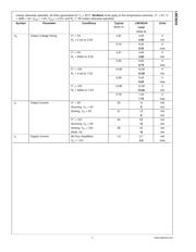
AC Electrical Characteristics
Unless otherwise specified, all limits guaranteed for T
J
= 25˚C. Boldface limits apply at the temperature extremes. V
+
= 5V, V
−
= GND = 0V, V
CM
= 1.5V, V
OUT
= 2.5V, and R
L
>
1M unless otherwise specified.
Symbol Parameter Conditions Typical
(Note 5)
LMC6034I Units
Limit
(Note 6)
SR Slew Rate (Note 8) 1.1 0.8 V/µs
0.4 min
GBW Gain-Bandwidth Product 1.4 MHz
φ
M
Phase Margin 50 Deg
G
M
Gain Margin 17 dB
Amp-to-Amp Isolation (Note 9) 130 dB
e
n
Input-Referred Voltage Noise F = 1 kHz 22
i
n
Input-Referred Current Noise F = 1 kHz 0.0002
THD Total Harmonic Distortion F = 10 kHz, A
V
= −10
R
L
=2kΩ,V
O
=8V
PP
0.01 %
±
5V Supply
Note 1: Absolute Maximum Ratings indicate limits beyond which damage to the component may occur. Operating Ratings indicate conditions for which the device
is intended to be functional, but do not guarantee specific performance limits. For guaranteed specifications and test conditions, see the Electrical Characteristics.
The guaranteed specifications apply only for the test conditions listed.
Note 2: Applies to both single-supply and split-supply operation. Continuous short circuit operation at elevated ambient temperature and/or multiple Op Amp shorts
can result in exceeding the maximum allowed junction temperature of 150˚C. Output currents in excess of
±
30 mA over long term may adversely affect reliability.
Note 3: The maximum power dissipation is a function of T
J(max)
, θ
JA
,T
A
. The maximum allowable power dissipation at any ambient temperature is P
D
=
(T
J(max)
–T
A
)/θ
JA
.
Note 4: Human body model, 100 pF discharged through a 1.5 kΩ resistor.
Note 5: Typical values represent the most likely parametric norm.
Note 6: All limits are guaranteed at room temperature (standard type face) or at operating temperature extremes (bold type face).
Note 7: V
+
= 15V, V
CM
= 7.5V, and R
L
connected to 7.5V. For Sourcing tests, 7.5V ≤ V
O
≤ 11.5V. For Sinking tests, 2.5V ≤ V
O
≤ 7.5V.
Note 8: V
+
= 15V. Connected as Voltage Follower with 10V step input. Number specified is the slower of the positive and negative slew rates.
Note 9: Input referred. V
+
= 15V and R
L
=10kΩ connected to V
+
/2. Each amp excited in turn with 1 kHz to produce V
O
=13V
PP
.
Note 10: Do not connect output to V
+
, when V
+
is greater than 13V or reliability may be adversely affected.
Note 11: For operating at elevated temperatures the device must be derated based on the thermal resistance θ
JA
with P
D
=(T
J
−T
A
)/θ
JA
.
Note 12: All numbers apply for packages soldered directly into a PC board.
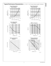
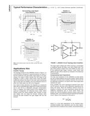
Typical Performance Characteristics
V
S
=
±
7.5V, T
A
= 25˚C unless otherwise specified
Supply Current
vs Supply Voltage Input Bias Current
01113423
01113424
LMC6034
www.national.com 4
器件 Datasheet 文档搜索
AiEMA 数据库涵盖高达 72,405,303 个元件的数据手册,每天更新 5,000 多个 PDF 文件
