Datasheet 搜索 > 运算放大器 > TI(德州仪器) > LMC6034IMX/NOPB 数据手册 > LMC6034IMX/NOPB 其他数据使用手册 6/13 页

 器件3D模型
¥ 5.084
LMC6034IMX/NOPB 其他数据使用手册 - TI(德州仪器)
制造商:
TI(德州仪器)
分类:
运算放大器
封装:
SOIC-14
描述:
四路 15.5V、1.4MHz、CMOS 运算放大器 14-SOIC -40 to 85
Pictures:
3D模型
符号图
焊盘图
引脚图
产品图
页面导航:

导航目录
LMC6034IMX/NOPB数据手册
Page:
of 13 Go
若手册格式错乱,请下载阅览PDF原文件
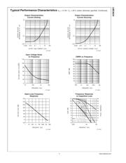
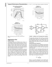
Typical Performance Characteristics V
S
=
±
7.5V, T
A
= 25˚C unless otherwise specified (Continued)
Non-Inverting Large Signal
Pulse Response
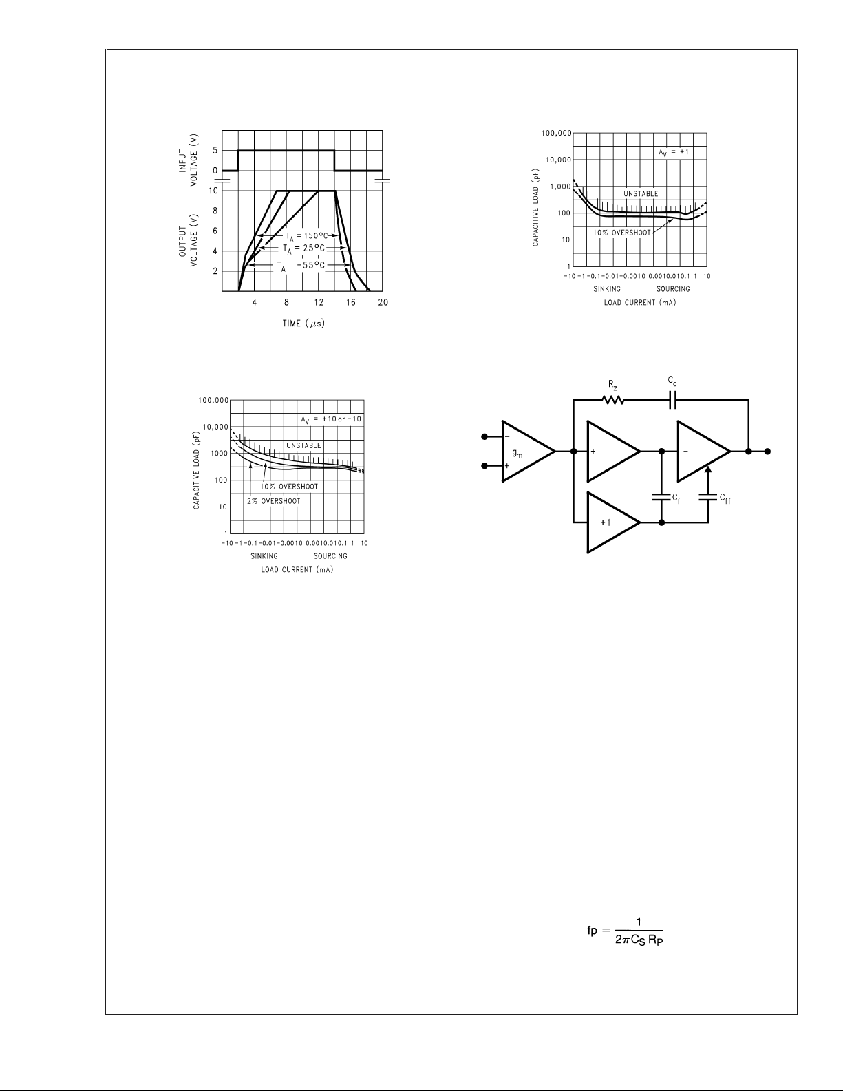
Stability vs
Capacitive Load
01113432
01113433
Stability vs
Capacitive Load
01113434
Note: Avoid resistive loads of less than 500Ω, as they may cause
instability.
Applications Hint
Amplifier Topolgy
The topology chosen for the LMC6034, shown in Figure 1,is
unconventional (compared to general-purpose op amps) in
that the traditional unity-gain buffer output stage is not used;
instead, the output is taken directly from the output of the
integrator, to allow a larger output swing. Since the buffer
traditionally delivers the power to the load, while maintaining
high op amp gain and stability, and must withstand shorts to
either rail, these tasks now fall to the integrator.
As a result of these demands, the integrator is a compound
affair with an embedded gain stage that is doubly fed forward
(via C
f
and Cff) by a dedicated unity-gain compensation
driver. In addition, the output portion of the integrator is a
push-pull configuration for delivering heavy loads. While
sinking current the whole amplifier path consists of three
gain stages with one stage fed forward, whereas while
sourcing the path contains four gain stages with two fed
forward.
The large signal voltage gain while sourcing is comparable
to traditional bipolar op amps, even with a 600Ω load. The
gain while sinking is higher than most CMOS op amps, due
to the additional gain stage; however, under heavy load
(600Ω) the gain will be reduced as indicated in the Electrical
Characteristics.
Compensating Input Capacitance
The high input resistance of the LMC6034 op amps allows
the use of large feedback and source resistor values without
losing gain accuracy due to loading. However, the circuit will
be especially sensitive to its layout when these large-value
resistors are used.
Every amplifier has some capacitance between each input
and AC ground, and also some differential capacitance be-
tween the inputs. When the feedback network around an
amplifier is resistive, this input capacitance (along with any
additional capacitance due to circuit board traces, the
socket, etc.) and the feedback resistors create a pole in the
feedback path. In the following General Operational Amplifier
circuit, Figure 2 the frequency of this pole is
where C
S
is the total capacitance at the inverting input,
including amplifier input capcitance and any stray capaci-
tance from the IC socket (if one is used), circuit board traces,
01113403
FIGURE 1. LMC6034 Circuit Topology (Each Amplifier)
LMC6034
www.national.com 6
器件 Datasheet 文档搜索
AiEMA 数据库涵盖高达 72,405,303 个元件的数据手册,每天更新 5,000 多个 PDF 文件
