Datasheet 搜索 > 运算放大器 > TI(德州仪器) > LMC6464BIMX/NOPB 数据手册 > LMC6464BIMX/NOPB 产品手册 3/18 页

 器件3D模型
¥ 16.545
LMC6464BIMX/NOPB 产品手册 - TI(德州仪器)
制造商:
TI(德州仪器)
分类:
运算放大器
封装:
SOIC-14
描述:
LMC6464BIMX/NOPB 编带
Pictures:
3D模型
符号图
焊盘图
引脚图
产品图
页面导航:
导航目录
LMC6464BIMX/NOPB数据手册
Page:
of 18 Go
若手册格式错乱,请下载阅览PDF原文件
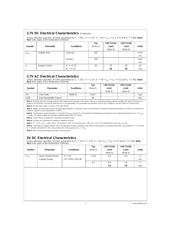
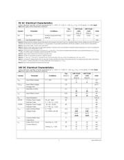
2.7V DC Electrical Characteristics (Continued)
Unless otherwise specified, all limits guaranteed for T
J
=
25˚C, V
+
=
2.7V, V
−
=
0V, V
CM
=
V
O
=
V
+
/2 and R
L
>
1MΩ.Bold-
face limits apply at the temperature extremes.
Typ LMC7111AI LMC7111BI
Symbol Parameter Conditions (Note 5) Limit Limit Units
(Note 6) (Note 6)
A
VOL
Voltage Gain Sourcing 400 V/mv
min
Sinking 150 V/mv
min
I
S
Supply Current V
+
=
+2.7V, 20 45 50 µA
V
O
=
V
+
/2 60 65 max
2.7V AC Electrical Characteristics
Unless otherwise specified, all limits guaranteed for T
J
=
25˚C, V
+
=
2.7V, V
−
=
0V, V
CM
=
V
O
=
V
+
/2 and R
L
>
1MΩ.Bold-
face limits apply at the temperature extremes.
Typ LMC7111AI LMC7111BI
Symbol Parameter Conditions (Note 5) Limit Limit Units
(Note 6) (Note 6)
SR Slew Rate (Note 8) 0.015 V/µs
GBW Gain-Bandwidth Product 40 kHz
Note 1: Absolute Maximum Ratings indicate limits beyond which damage to the device may occur. Operating Ratings indicate conditions for which the device is in-
tended to be functional, but specific performance is not guaranteed. For guaranteed specifications and the test conditions, see the Electrical Characteristics.
Note 2: Human body model, 1.5 kΩ in series with 100 pF.
Note 3: Applies to both single-supply and split-supply operation. Continuous short circuit operation at elevated ambient temperature can result in exceeding the
maximum allowed junction temperature at 150˚C.
Note 4: The maximum power dissipation is a function ofT
J(max)
, θ
JA
and T
A
. The maximum allowable power dissipation at any ambient temperature is P
D
=
(T
J(max)
−T
A
)/θ
JA
. All numbers apply for packages soldered directly into a PC board.
Note 5: Typical Values represent the most likely parametric norm.
Note 6: All limits are guaranteed by testing or statistical analysis.
Note 7: V
+
=
2.7V, V
CM
=
1.35V and R
L
connected to 1.35V. For Sourcing tests, 1.35V ≤ V
O
≤ 2.7V. For Sinking tests, 0.5V ≤ V
O
≤ 1.35V.
Note 8: Connected as Voltage Follower with 1.0V step input. Number specified is the slower of the positive and negative slew rates. Input referred, V
+
=
2.7V and
R
L
=
100 kΩ connected to 1.35V. Amp excited with 1 kHz to produce V
O
=
1V
PP
.
Note 9: Bias Current guaranteed by design and processing.
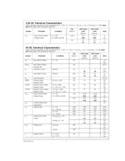
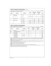
3V DC Electrical Characteristics
Unless otherwise specified, all limits guaranteed for T
J
=
25˚C, V
+
=
3V, V
−
=
0V, V
CM
=
V
O
=
V
+
/2 and R
L
>
1MΩ.Bold-
face limits apply at the temperature extremes.
Typ LMC7111AI LMC7111BI
Symbol Parameter Conditions (Note 5) Limit Limit Units
(Note 6) (Note 6)
V
CM
Input Common-Mode V
+
=
3V −0.25 0.0 0.0 V
Voltage Range For CMRR ≥ 50 dB min
3.2 3.0 3.0 V
2.8 2.8 max
www.national.com3
器件 Datasheet 文档搜索
AiEMA 数据库涵盖高达 72,405,303 个元件的数据手册,每天更新 5,000 多个 PDF 文件
