Datasheet 搜索 > 运算放大器 > TI(德州仪器) > LMC6464BIMX/NOPB 数据手册 > LMC6464BIMX/NOPB 产品手册 5/18 页

 器件3D模型
¥ 16.545
LMC6464BIMX/NOPB 产品手册 - TI(德州仪器)
制造商:
TI(德州仪器)
分类:
运算放大器
封装:
SOIC-14
描述:
LMC6464BIMX/NOPB 编带
Pictures:
3D模型
符号图
焊盘图
引脚图
产品图
页面导航:
导航目录
LMC6464BIMX/NOPB数据手册
Page:
of 18 Go
若手册格式错乱,请下载阅览PDF原文件
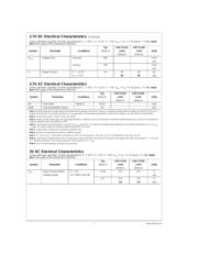
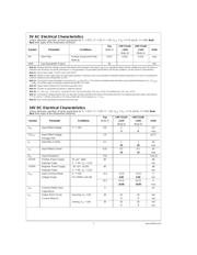
5V AC Electrical Characteristics
Unless otherwise specified, all limits guaranteed for T
J
=
25˚C, V
+
=
5V, V
−
=
0V, V
CM
=
V
O
=
V
+
/2 and R
L
>
1MΩ.Bold-
face limits apply at the temperature extremes.
Typ LMC7111AI LMC7111BI
Symbol Parameter Conditions (Note 5) Limit Limit Units
(Note 6) (Note 6)
SR Slew Rate Positive Going Slew Rate 0.027 0.015 0.010 V/µs
(Note 8)
GBW Gain-Bandwidth Product 50 kHz
Note 10: Absolute Maximum Ratings indicate limits beyond which damage to the device may occur. Operating Ratings indicate conditions for which the device is
intended to be functional, but specific performance is not guaranteed. For guaranteed specifications and the test conditions, see the Electrical Characteristics.
Note 11: Human body model, 1.5 kΩ in series with 100 pF.
Note 12: Applies to both single-supply and split-supply operation. Continuous short circuit operation at elevated ambient temperature can result in exceeding the
maximum allowed junction temperature at 150˚C.
Note 13: The maximum power dissipationisa function of T
J(max)
, θ
JA
and T
A
. The maximum allowablepowerdissipationat any ambient temperatureisP
D
=
(T
J(max)
−T
A
)/θ
JA
. All numbers apply for packages soldered directly into a PC board.
Note 14: Typical Values represent the most likely parametric norm.
Note 15: All limits are guaranteed by testing or statistical analysis.
Note 16: V
+
=
5V, V
CM
=
2.5V and R
L
connected to 2.5V. For Sourcing tests, 2.5V ≤ V
O
≤ 5.0V. For Sinking tests, 0.5V ≤ V
O
≤ 2.5V.
Note 17: Connected as Voltage Follower with1.0Vstep input. Number specifiedisthe slower of the positiveslewrate.Thenegative slew rate isfaster. Inputreferred,
V
+
=
5V and R
L
=
100 kΩ connected to 1.5V. Amp excited with 1 kHz to produce V
O
=
1V
PP
.
Note 18: Bias Current guaranteed by design and processing.
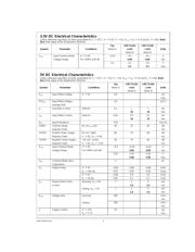
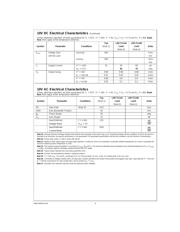
10V DC Electrical Characteristics
Unless otherwise specified, all limits guaranteed for T
J
=
25˚C, V
+
=
10V, V
−
=
0V, V
CM
=
V
O
=
V
+
/2 and R
L
>
1MΩ.Bold-
face limits apply at the temperature extremes.
Typ LMC7111AI LMC7111BI
Symbol Parameter Conditions (Note 5) Limit Limit Units
(Note 6) (Note 6)
V
OS
Input Offset Voltage V
+
=
10V 0.9 3 7 mV
59max
TCV
OS
Input Offset Voltage 2.0 µV/˚C
Average Drift
I
B
Input Bias Current 0.1 1 1 pA
20 20 max
I
OS
Input Offset Current 0.01 0.5 0.5 pA
10 10 max
R
IN
Input Resistance
>
10 Tera Ω
+PSRR Positive Power Supply 5V ≤ V
+
≤10V, 80 dB
Rejection Ratio V
−
=
0V, V
O
=
2.5V min
−PSRR Negative Power Supply −5V ≤ V
−
≤−10V, 80 dB
Rejection Ratio V
−
=
0V, V
O
=
2.5V min
V
CM
Input Common-Mode V
+
=
10V −0.2 −0.15 −0.15 V
Voltage Range For CMRR ≥ 50 dB 0.00 0.00 min
10.2 10.15 10.15 V
10.00 10.00 max
C
IN
Common-Mode Input 3 pF
Capacitance
I
SC
Output Short Circuit Sourcing, V
O
=
0V 30 20 20 mA
Current (Note 9) 77min
Sinking, V
O
=
10V 30 20 20 mA
77min
www.national.com5
器件 Datasheet 文档搜索
AiEMA 数据库涵盖高达 72,405,303 个元件的数据手册,每天更新 5,000 多个 PDF 文件
