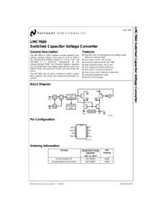
Datasheet 搜索 > 稳压芯片 > National Semiconductor(美国国家半导体) > LMC7660IMX 数据手册 > LMC7660IMX 产品手册 2/12 页

 器件3D模型
¥ 2.848
LMC7660IMX 产品手册 - National Semiconductor(美国国家半导体)
制造商:
National Semiconductor(美国国家半导体)
分类:
稳压芯片
封装:
PDIP
描述:
LMC7660IMX
Pictures:
3D模型
符号图
焊盘图
引脚图
产品图
页面导航:
导航目录
LMC7660IMX数据手册
Page:
of 12 Go
若手册格式错乱,请下载阅览PDF原文件
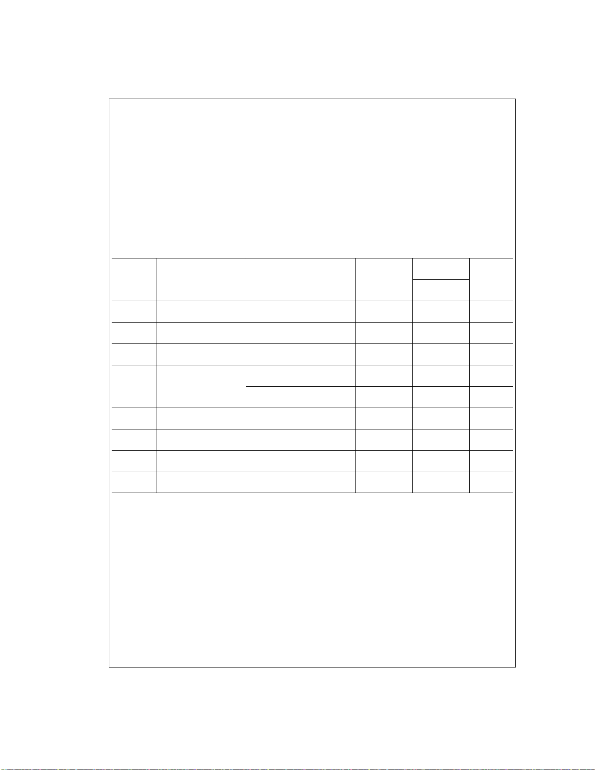
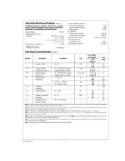
Absolute Maximum Ratings (Note 1)
If Military/Aerospace specified devices are required,
please contact the National Semiconductor Sales Office/
Distributors for availability and specifications.
Supply Voltage 10.5V
Input Voltage on Pin 6, 7
(Note 2) −0.3V to (V
+
+ 0.3V)
for V
+
<
5.5V
(V
+
− 5.5V) to (V
+
+ 0.3V)
for V
+
>
5.5V
Current into Pin 6 (Note 2) 20 µA
Output Short Circuit
Duration (V
+
≤ 5.5V) Continuous
Power Dissipation (Note 3)
Dual-In-Line Package 1.4W
Surface-Mount Package 0.6W
T
J
Max (Note 3) 150˚C
θ
JA
(Note 3)
Dual-In-Line Package 90˚C/W
Surface-Mount Package 160˚C/W
Storage Temp. Range −65˚C ≤ T ≤ 150˚C
Lead Temperature
(Soldering, 5 sec.) 260˚C
ESD Tolerance (Note 7)
±
2000V
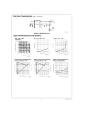
Electrical Characteristics (Note 4)
Symbol Parameter Conditions Typ
LMC7660IN/
Units
Limits
LMC7660IM
Limit
(Note 5)
I
s
Supply Current R
L
=
∞
120 200 µA
400 max
V
+
H Supply Voltage R
L
=
10 kΩ, Pin 6 Open 3 to 10 3 to 10 V
Range High (Note 6) Voltage Efficiency ≥ 90
%
3to10
V
+
L Supply Voltage R
L
=
10 kΩ, Pin 6 to Gnd. 1.5 to 3.5 1.5 to 3.5 V
Range Low Voltage Efficiency ≥ 90
%
1.5 to 3.5
R
out
Output Source I
L
=
20 mA 55 100 Ω
Resistance 120 max
V
=
2V, I
L
=
3 mA 110 200 Ω
Pin 6 Short to Gnd. 300 max
F
osc
Oscillator 10 kHz
Frequency
P
eff
Power Efficiency R
L
=
5kΩ 97 95
%
90 min
V
o eff
Voltage Conversion R
L
=
∞
99.9 97
%
Efficiency 95 min
I
osc
Oscillator Sink or Pin 7
=
Gnd. or V
+
3µA
Source Current
Note 1: Absolute Maximum ratings indicate limits beyond which damage to the device may occur. DC and AC electrical specifications do not apply when operating
the device beyond its rated operating conditions. See Note 4 for conditions.
Note 2: Connecting any input terminal to voltages greater than V
+
or less than ground may cause destructive latchup. It is recommended that no inputs from sources
operating from external supplies be applied prior to “power-up” of the LMC7660.
Note 3: For operation at elevated temperature, these devices must be derated based on a thermal resistance of θ
ja
and T
j
max, T
j
=
T
A
+ θ
ja
P
D
.
Note 4: Boldface numbers apply at temperature extremes. All other numbers apply at T
A
=
25˚C, V
+
=
5V, C
osc
=
0, and apply for the LMC7660 unless otherwise
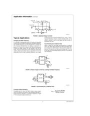
specified. Test circuit is shown in
Figure 1
.
Note 5: Limits at room temperature are guaranteed and 100
%
production tested. Limits in boldface are guaranteed over the operating temperature range (but not
100
%
tested), and are not used to calculate outgoing quality levels.
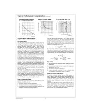
Note 6: The LMC7660 can operate without an external diode over the full temperature and voltage range. The LMC7660 can also be used with the external diode
Dx, when replacing previous 7660 designs.
Note 7: The test circuit consists of the human body model of 100 pF in series with 1500Ω.
www.national.com 2
器件 Datasheet 文档搜索
AiEMA 数据库涵盖高达 72,405,303 个元件的数据手册,每天更新 5,000 多个 PDF 文件
