Datasheet 搜索 > DC/DC转换器 > TI(德州仪器) > LMZ31704RVQR 数据手册 > LMZ31704RVQR 产品封装文件 3/33 页

¥ 54.816
LMZ31704RVQR 产品封装文件 - TI(德州仪器)
制造商:
TI(德州仪器)
分类:
DC/DC转换器
封装:
QFN-42
描述:
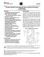
4A SIMPLE SWITCHER®电源模块具有2.95V - 17V输入和电流共享的QFN封装 4A SIMPLE SWITCHER® Power Module with 2.95V-17V Input and Current Sharing in QFN Package
Pictures:
3D模型
符号图
焊盘图
引脚图
产品图
页面导航:
引脚图在P6P7Hot
原理图在P5P15P16P17P23
封装尺寸在P27
焊盘布局在P6
型号编码规则在P2
标记信息在P27
封装信息在P2P27P28
技术参数、封装参数在P2
应用领域在P1P16P17P33
电气规格在P3P4
导航目录
LMZ31704RVQR数据手册
Page:
of 33 Go
若手册格式错乱,请下载阅览PDF原文件
LMZ31704
www.ti.com
SLVSBV8A –JUNE 2013–REVISED AUGUST 2013
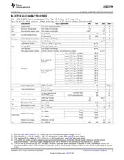
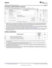
ELECTRICAL CHARACTERISTICS
Over –40°C to 85°C free-air temperature, PV
IN
= V
IN
= 12 V, V
OUT
= 1.8 V, I
OUT
= 4 A,
C
IN
= 0.1 µF + 2 x 22 µF ceramic + 100 µF bulk, C
OUT
= 4 x 47 µF ceramic (unless otherwise noted)
PARAMETER TEST CONDITIONS MIN TYP MAX UNIT
I
OUT
Output current T
A
= 85°C, natural convection 0
(1)
4 A
V
IN
Input bias voltage range Over output current range 4.5 17 V
PV
IN
Input switching voltage range Over output current range 2.95
(2)
17
(3)
V
V
IN
Increasing 4.0 4.5
UVLO V
IN
Undervoltage lockout V
V
IN
Decreasing 3.5 3.85
V
OUT(adj)
Output voltage adjust range Over output current range 0.6 5.5 V
Set-point voltage tolerance T
A
= 25°C, I
OUT
= 0 A ±1%
(4)
Temperature variation –40°C ≤ T
A
≤ +85°C, I
OUT
= 0 A ±0.2%
V
OUT
Line regulation Over input voltage range ±0.1%
Load regulation Over output current range ±0.2%
Total output voltage variation Includes set-point, line, load, and temperature variation ±1.5%
(4)
V
OUT
= 5.0 V, f
SW
= 1 MHz 94 %
V
OUT
= 3.3 V, f
SW
= 750 kHz 92 %
V
OUT
= 2.5 V, f
SW
= 750 kHz 89 %
P
VIN
= V
IN
= 12 V
V
OUT
= 1.8 V, f
SW
= 500 kHz 88 %
I
O
= 3 A
V
OUT
= 1.2 V, f
SW
= 300 kHz 86 %
V
OUT
= 0.9 V, f
SW
= 250 kHz 84 %
η Efficiency V
OUT
= 0.6 V, f
SW
= 200 kHz 81 %
P
VIN
= V
IN
= 5 V V
OUT
= 3.3 V, f
SW
= 750 kHz 95 %
I
O
= 3 A
V
OUT
= 2.5 V, f
SW
= 750 kHz 94 %
V
OUT
= 1.8 V, f
SW
= 500 kHz 93 %
V
OUT
= 1.2 V, f
SW
= 300 kHz 91 %
V
OUT
= 0.9 V, f
SW
= 250 kHz 89 %
V
OUT
= 0.6 V, f
SW
= 200 kHz 86 %
Output voltage ripple 20 MHz bandwith 14 mV
P-P
ILIM pin open 9 A
I
LIM
Current limit threshold
ILIM pin to AGND 6 A
Recovery time 100 µs
1.0 A/µs load step from
Transient response
25 to 75% I
OUT(max)
VOUT over/undershoot 80 mV
Inhibit High Voltage 1.3 open
(5)
V
INH
Inhibit threshold voltage V
Inhibit Low Voltage -0.3 1.1
INH Input current V
INH
< 1.1 V -1.15 μA
I
INH
INH Hysteresis current V
INH
> 1.3 V -3.3 μA
I
I(stby)
Input standby current INH pin to AGND 2 10 µA
Good 95%
V
OUT
rising
Fault 108%
PWRGD Thresholds
Power Good Fault 91%
V
OUT
falling
Good 104%
PWRGD Low Voltage I(PWRGD) = 0.5 mA 0.3 V
f
SW
Switching frequency R
RT
= 169 kΩ 400 500 600 kHz
(1) See the Light Load Efficiency (LLE) section for more information for output voltages < 1.5 V.
(2) The minimum P
VIN
is 2.95 V or (V
OUT
+ 0.7 V), whichever is greater. See Table 9 for more details.
(3) The maximum PV
IN
voltage is 17 V or (22 x V
OUT
), whichever is less. See Table 9 for more details.
(4) The stated limit of the set-point voltage tolerance includes the tolerance of both the internal voltage reference and the internal
adjustment resistor. The overall output voltage tolerance will be affected by the tolerance of the external R
SET
resistor.
(5) This pin has an internal pull-up. If it is left open, the device operates when input power is applied. A small, low-leakage MOSFET is
recommended for control. When the device is operating and no UVLO resistor divider is present on this pin, the open voltage is typically
2.9 V.
Copyright © 2013, Texas Instruments Incorporated Submit Documentation Feedback 3
Product Folder Links: LMZ31704
器件 Datasheet 文档搜索
AiEMA 数据库涵盖高达 72,405,303 个元件的数据手册,每天更新 5,000 多个 PDF 文件
