Datasheet 搜索 > 接口芯片 > Maxim Integrated(美信) > MAX3096CSE+ 数据手册 > MAX3096CSE+ 其他数据使用手册 2/12 页
 器件3D模型
¥ 31.289
MAX3096CSE+ 其他数据使用手册 - Maxim Integrated(美信)
制造商:
Maxim Integrated(美信)
分类:
接口芯片
封装:
SOIC-16
描述:
RS-485 多通道发射器/接收器,Maxim Integrated### RS-485 线路驱动器和接收器
Pictures:
3D模型
符号图
焊盘图
引脚图
产品图
页面导航:
导航目录
MAX3096CSE+数据手册
Page:
of 12 Go
若手册格式错乱,请下载阅览PDF原文件
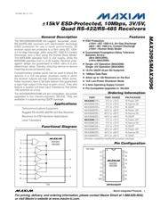
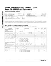
MAX3095/MAX3096
±15kV ESD-Protected, 10Mbps, 3V/5V,
Quad RS-422/RS-485 Receivers
2 _______________________________________________________________________________________
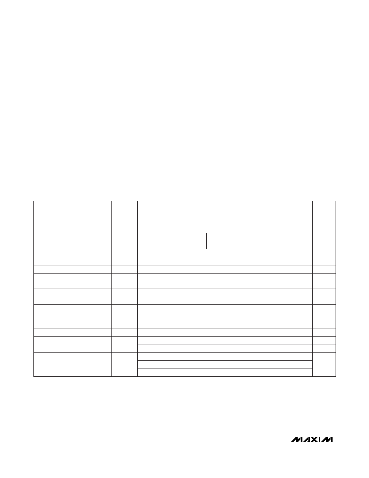
ABSOLUTE MAXIMUM RATINGS
DC ELECTRICAL CHARACTERISTICS—MAX3095
(V
CC
= 5V ±5%, T
A
= T
MIN
to T
MAX
, unless otherwise noted. Typical values are at T
A
= +25°C.) (Note 1)
Stresses beyond those listed under “Absolute Maximum Ratings” may cause permanent damage to the device. These are stress ratings only, and functional
operation of the device at these or any other conditions beyond those indicated in the operational sections of the specifications is not implied. Exposure to
absolute maximum rating conditions for extended periods may affect device reliability.
Supply Voltage (V
CC
)...............................................................7V
Control Input Voltage (G, G).......................-0.3V to (V
CC
+ 0.3V)
Receiver Input Voltage (A_, B_)...........................................±25V
Receiver Output Voltage (Y_).....................-0.3V to (V
CC
+ 0.3V)
Continuous Power Dissipation (T
A
= +70°C)
16-Pin Plastic DIP (derate 10.5mW/°C above +70°C) .762mW
16-Pin SO (derate 8.7mW/°C above +70°C)................696mW
16-Pin QSOP (derate 8.3mW/°C above +70°C)...........667mW
Operating Temperature Ranges
MAX309_C_ _ .....................................................0°C to +70°C
MAX309_E_ _...................................................-40°C to +85°C
Storage Temperature Range .............................-65°C to +160°C
Lead Temperature (soldering, 10s) .................................+300°C
V
CM
= 0V
IEC 1000-4-2 (Contact Discharge)
-7V ≤ V
CM
≤ 12V
IEC 1000-4-2 (Air-Gap Discharge)
Human Body Model
-7V ≤ V
CM
≤ 12V
0 ≤ V
OUT
≤ V
CC
, G = V
CC
or G = GND
0 ≤ V
OUT
≤ V
CC
, G = GND and G = V
CC
I
OUT
= 4mA, V
ID
= -200mV,
G = V
CC
or G = GND, Figure 1
G = GND and G = V
CC
I
OUT
= -4mA, V
ID
= 200mV,
G = V
CC
or G = GND, Figure 1
No load, G = V
CC
or G = GND
CONDITIONS
±8
±15
kV
±15
ESD Protection
(Note 2)
µA0.001 10
mA2.4 3.5
I
CC
Supply Current
mV45
mV-200 200V
TH
Receiver Differential Input
Threshold
Receiver Input Hysteresis
kΩ48R
IN
Receiver Input Resistance
mA±7 ±75I
OSR
Output Short-Circuit Current
µA±1I
OZR
Three-State Current at Receiver
Output
V0.4V
OL
Receiver Output Low Voltage
µA±1
Enable Input Current (G, G)
V2.0V
IH
Enable Input High Voltage (G, G)
V0.8V
IL
Enable Input Low Voltage (G, G)
VV
CC
- 1.5V
OH
Receiver Output High Voltage
UNITSMIN TYP MAXSYMBOLPARAMETER
µA
250
I
IN
Receiver Input Current (A_, B_) V
CC
= 0V or 5.25V
V
IN
= 12V
-200V
IN
= -7V
器件 Datasheet 文档搜索
AiEMA 数据库涵盖高达 72,405,303 个元件的数据手册,每天更新 5,000 多个 PDF 文件
