Datasheet 搜索 > 接口芯片 > Maxim Integrated(美信) > MAX3096CSE+ 数据手册 > MAX3096CSE+ 其他数据使用手册 6/12 页
 器件3D模型
¥ 31.3
MAX3096CSE+ 其他数据使用手册 - Maxim Integrated(美信)
制造商:
Maxim Integrated(美信)
分类:
接口芯片
封装:
SOIC-16
描述:
RS-485 多通道发射器/接收器,Maxim Integrated### RS-485 线路驱动器和接收器
Pictures:
3D模型
符号图
焊盘图
引脚图
产品图
页面导航:
导航目录
MAX3096CSE+数据手册
Page:
of 12 Go
若手册格式错乱,请下载阅览PDF原文件
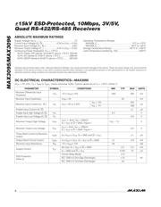
MAX3095/MAX3096
±15kV ESD-Protected, 10Mbps, 3V/5V,
Quad RS-422/RS-485 Receivers
6 _______________________________________________________________________________________
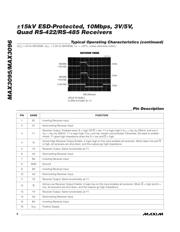
_ Pin Description
NAME FUNCTION
1 B1 Inverting Receiver Input
2 A1 Noninverting Receiver Input
PIN
3 Y1
Receiver Output. Enabled when G = high OR G = low. Y1 is logic-high if V
A1
> V
B1
by 200mV, and low if
V
A1
< V
B1
by 200mV. Y1 is logic-high if V
A1
and V
B1
remain unconnected. Otherwise, the state is undeter-
mined. Y1 goes high impedance when the G = low
and
G = high.
4 G
Active-High Receiver Output Enable. A logic-high on this input enables all receivers. When taken low and G
is high, all receivers are shut down, and the outputs go high impedance.
8 GND Ground
7 B2 Inverting Receiver Input
6 A2 Noninverting Receiver Input
5 Y2 Receiver Output. Same functionality as Y1.
13 Y4 Receiver Output. Same functionality as Y1.
12
G
Active-Low Receiver Output Enable. A logic-low on this input enables all receivers. When G = high and G =
low, all receivers are shut down, and the outputs go high impedance.
11 Y3 Receiver Output. Same functionality as Y1.
10 A3 Noninverting Receiver Input
9 B3 Inverting Receiver Input
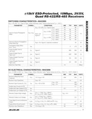
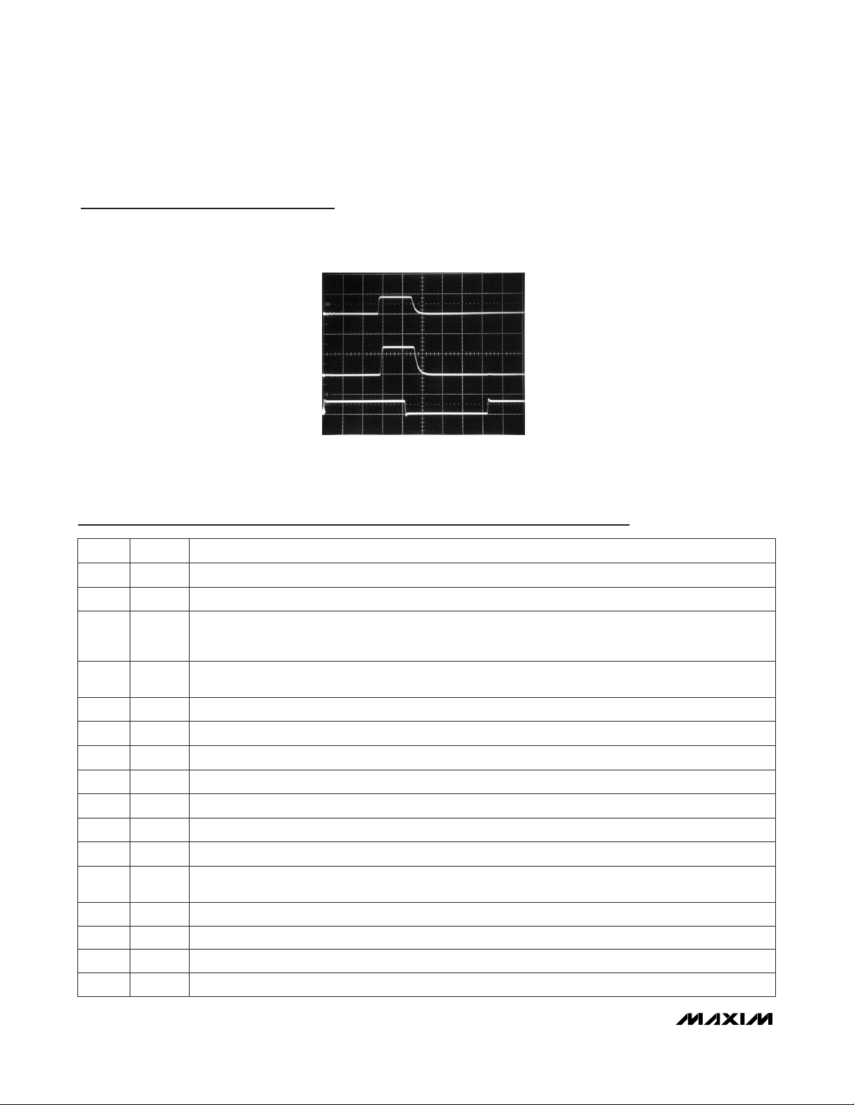
TIME (200ns/div)
SHUTDOWN TIMING
MAX3095 TOC09
MAX3095
Y VOLTAGE
5V/div
2V/div
2V/div
MAX3096
Y VOLTAGE
G VOLTAGE
CIRCUIT OF FIGURE 3,
S1 OPEN, S2 CLOSED, S3 = 1V
Typical Operating Characteristics (continued)
(V
CC
= 5V for MAX3095, V
CC
= 3.3V for MAX3096, T
A
= +25°C, unless otherwise noted.)
14 A4 Noninverting Receiver Input
15 B4 Inverting Receiver Input
16 V
CC
Positive Supply
器件 Datasheet 文档搜索
AiEMA 数据库涵盖高达 72,405,303 个元件的数据手册,每天更新 5,000 多个 PDF 文件
