Datasheet 搜索 > 接口芯片 > TI(德州仪器) > MAX3243CDB 数据手册 > MAX3243CDB 其他数据使用手册 4/19 页
 器件3D模型
¥ 2.645
MAX3243CDB 其他数据使用手册 - TI(德州仪器)
制造商:
TI(德州仪器)
分类:
接口芯片
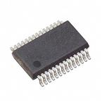
封装:
SSOP-28
描述:
TEXAS INSTRUMENTS MAX3243CDB. 线路接收器, RS232, 3驱动器, 3V-5.5电源, SSOP-28
Pictures:
3D模型
符号图
焊盘图
引脚图
产品图
页面导航:
封装尺寸在P12P13P14P15
封装信息在P12P13P14P15
应用领域在P13P19
导航目录
MAX3243CDB数据手册
Page:
of 19 Go
若手册格式错乱,请下载阅览PDF原文件
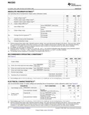
ABSOLUTE MAXIMUM RATINGS
(1)
RECOMMENDED OPERATING CONDITIONS
(1)
ELECTRICAL CHARACTERISTICS
(1)
MAX3243
SLLS350M – APRIL 1999 – REVISED SEPTEMBER 2008 ................................................................................................................................................
www.ti.com
over operating free-air temperature range (unless otherwise noted)
MIN MAX UNIT
V
CC
Supply voltage range
(2)
– 0.3 6 V
V+ Positive output supply voltage range
(2)
– 0.3 7 V
V – Negative output supply voltage range
(2)
0.3 – 7 V
V+ – V – Supply voltage difference
(2)
13 V
Driver ( FORCEOFF, FORCEON) – 0.3 6
V
I
Input voltage range V
Receiver – 25 25
Driver – 13.2 13.2
V
O
Output voltage range V
Receiver ( INVALID) – 0.3 V
CC
+ 0.3
DB package 62
θ
JA
Package thermal impedance
(3) (4)
DW package 46 ° C/W
PW package 62
T
J
operating virutal junction temperature 150 ° C
T
stg
Storage temperature range – 65 150 ° C
(1) Stresses beyond those listed under " absolute maximum ratings " may cause permanent damage to the device. These are stress ratings
only, and functional operation of the device at these or any other conditions beyond those indicated under " recommended operating
conditions " is not implied. Exposure to absolute-maximum-rated conditions for extended periods may affect device reliability.
(2) All voltages are with respect to network GND.
(3) Maximum power dissipation is a function of T
J
(max), θ
JA
, and T
A
. The maximum allowable power dissipation at any allowable ambient
temperature is P
D
= (T
J
(max) - T
A
)/ θ
JA
. Operating at the absolute maximum T
J
of 150 ° C can affect reliability.
(4) The package thermal impedance is calculated in accordance with JESD 51-7.
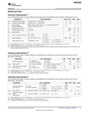
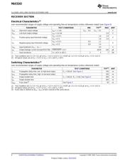
See Figure 6
MIN NOM MAX UNIT
V
CC
= 3.3 V 3 3.3 3.6
Supply voltage V
V
CC
= 5 V 4.5 5 5.5
V
CC
= 3.3 V 2
DIN, FORCEOFF,
V
IH
Driver and control high-level input voltage V
FORCEON
V
CC
= 5 V 2.4
V
IL
Driver and control low-level input voltage DIN, FORCEOFF, FORCEON 0.8 V
V
I
Driver and control input voltage DIN, FORCEOFF, FORCEON 0 5.5 V
V
I
Receiver input voltage – 25 25 V
MAX3243C, MAX3243FC 0 70
T
A
Operating free-air temperature ° C
MAX3243I, MAX3243FI – 40 85
(1) Test conditions are C1 – C4 = 0.1 µ F at V
CC
= 3.3 V ± 0.3 V; C1 = 0.047 µ F, C2 – C4 = 0.33 µ F at V
CC
= 5 V ± 0.5 V.
over recommended ranges of supply voltage and operating free-air temperature (unless otherwise noted) (see Figure 6 )
PARAMETER TEST CONDITIONS MIN TYP
(2)
MAX UNIT
I
I
Input leakage current FORCEOFF, FORCEON ± 0.01 ± 1 µ A
No load,
Auto-powerdown disabled 0.3 1 mA
FORCEOFF and FORCEON at V
CC
Powered off No load, FORCEOFF at GND 1 10
Supply current
I
CC
No load, FORCEOFF at V
CC
,
(T
A
= 25 ° C)
µ A
FORCEON at GND,
Auto-powerdown enabled 1 10
All RIN are open or grounded,
All DIN are grounded
(1) Test conditions are C1 – C4 = 0.1 µ F at V
CC
= 3.3 V ± 0.3 V; C1 = 0.047 µ F, C2 – C4 = 0.33 µ F at V
CC
= 5 V ± 0.5 V.
(2) Stresses beyond those listed under " absolute maximum ratings " may cause permanent damage to the device. These are stress ratings
only, and functional operation of the device at these or any other conditions beyond those indicated under " recommended operating
conditions " is not implied. Exposure to absolute-maximum-rated conditions for extended periods may affect device reliability.
4 Submit Documentation Feedback Copyright © 1999 – 2008, Texas Instruments Incorporated
Product Folder Link(s): MAX3243
器件 Datasheet 文档搜索
AiEMA 数据库涵盖高达 72,405,303 个元件的数据手册,每天更新 5,000 多个 PDF 文件
