Datasheet 搜索 > 接口芯片 > TI(德州仪器) > MAX3243CDB 数据手册 > MAX3243CDB 其他数据使用手册 5/19 页
 器件3D模型
¥ 2.646
MAX3243CDB 其他数据使用手册 - TI(德州仪器)
制造商:
TI(德州仪器)
分类:
接口芯片
封装:
SSOP-28
描述:
TEXAS INSTRUMENTS MAX3243CDB. 线路接收器, RS232, 3驱动器, 3V-5.5电源, SSOP-28
Pictures:
3D模型
符号图
焊盘图
引脚图
产品图
页面导航:
封装尺寸在P12P13P14P15
封装信息在P12P13P14P15
应用领域在P13P19
导航目录
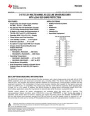
MAX3243CDB数据手册
Page:
of 19 Go
若手册格式错乱,请下载阅览PDF原文件
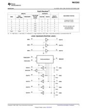
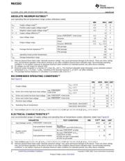
DRIVER SECTION
Electrical Characteristics
(1)
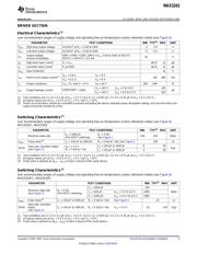
Switching Characteristics
(1)
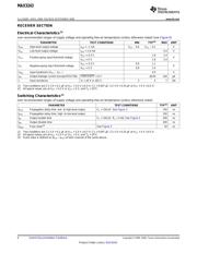
Switching Characteristics
(1)
MAX3243
www.ti.com
................................................................................................................................................ SLLS350M – APRIL 1999 – REVISED SEPTEMBER 2008
over recommended ranges of supply voltage and operating free-air temperature (unless otherwise noted) (see Figure 6 )
PARAMETER TEST CONDITIONS MIN TYP
(2)
MAX UNIT
V
OH
High-level output voltage All DOUT at R
L
= 3 k Ω to GND 5 5.4 V
V
OL
Low-level output voltage All DOUT at R
L
= 3 k Ω to GND – 5 – 5.4 V
Output voltage DIN1 = DIN2 = GND, DIN3 = V
CC
, 3-k Ω to GND at DOUT3,
V
O
± 5 V
(mouse driveability) DOUT1 = DOUT2 = 2.5 mA
I
IH
High-level input current V
I
= V
CC
± 0.01 ± 1 µ A
I
IL
Low-level input current V
I
at GND ± 0.01 ± 1 µ A
V
hys
Input hysteresis ± 1 V
V
CC
= 3.6 V, V
O
= 0 V
I
OS
Short-circuit output current
(3)
± 35 ± 60 mA
V
CC
= 5.5 V, V
O
= 0 V
r
o
Output resistance V
CC
, V+, and V – = 0 V, V
O
= ± 2 V 300 10M Ω
V
O
= ± 12 V, V
CC
= 3 to 3.6 V ± 25
I
off
Output leakage current FORCEOFF = GND, µ A
V
O
= ± 10 V, V
CC
= 4.5 to 5.5 V ± 25
(1) Test conditions are C1 – C4 = 0.1 µ F at V
CC
= 3.3 V ± 0.3 V; C1 = 0.047 µ F, C2 – C4 = 0.33 µ F at V
CC
= 5 V ± 0.5 V.
(2) All typical values are at V
CC
= 3.3 V or V
CC
= 5 V, and T
A
= 25 ° C.
(3) Short-circuit durations should be controlled to prevent exceeding the device absolute power dissipation ratings, and not more than one
output should be shorted at a time.
over recommended ranges of supply voltage and operating free-air temperature (unless otherwise noted) (see Figure 6 )
MAX3243C, MAX3243I
PARAMETER TEST CONDITIONS MIN TYP
(2)
MAX UNIT
C
L
= 1000 pF, R
L
= 3 k Ω
Maximum data rate 150 250 kbit/s
One DOUT switching, See Figure 1
t
sk(p)
Pulse skew
(3)
C
L
= 150 pF to 2500 pF, R
L
= 3 k Ω to 7 k Ω , See Figure 3 100 ns
C
L
= 150 pF to 1000 pF 6 30
Slew rate, transition region V
CC
= 3.3 V,
SR(tr) V/ µ s
(see Figure 1 ) R
L
= 3 k Ω to 7 k Ω
C
L
= 150 pF to 2500 pF 4 30
(1) Test conditions are C1 – C4 = 0.1 µ F at V
CC
= 3.3 V + 0.3 V; C1 = 0.047 µ F, C2 – C4 = 0.33 µ F at V
CC
= 5 V ± 0.5 V.
(2) All typical values are at V
CC
= 3.3 V or V
CC
= 5 V, and T
A
= 25 ° C.
(3) Pulse skew is defined as |t
PLH
– t
PHL
| of each channel of the same device.
over recommended ranges of supply voltage and operating free-air temperature (unless otherwise noted) (see Figure 6 )
MAX3243FC, MAX3243FI
PARAMETER TEST CONDITIONS MIN TYP
(2)
MAX UNIT
C
L
= 1000 pF 250
Maximum data rate R
L
= 3 k Ω
C
L
= 250 pF, V
CC
= 3 V to 4.5 V 1000 kbit/s
(see Figure 1 ) One DOUT switching,
C
L
= 1000 pF, V
CC
= 4.5 V to 4.5 V 1000
t
sk(p)
Pulse skew
(3)
C
L
= 150 pF to 2500 pF, R
L
= 3 k Ω to 7 k Ω , See Figure 2 25 ns
Slew rate, transition
SR(tr) region C
L
= 150 pF to 1000 pF, R
L
= 3 k Ω to 7 k Ω , V
CC
= 3.3 V 18 150 V/ µ s
(see Figure 1 )
(1) Test conditions are C1 – C4 = 0.1 µ F at V
CC
= 3.3 V + 0.3 V; C1 = 0.047 µ F, C2 – C4 = 0.33 µ F at V
CC
= 5 V ± 0.5 V.
(2) All typical values are at V
CC
= 3.3 V or V
CC
= 5 V, and T
A
= 25 ° C.
(3) Pulse skew is defined as |t
PLH
– t
PHL
| of each channel of the same device.
Copyright © 1999 – 2008, Texas Instruments Incorporated Submit Documentation Feedback 5
Product Folder Link(s): MAX3243
器件 Datasheet 文档搜索
AiEMA 数据库涵盖高达 72,405,303 个元件的数据手册,每天更新 5,000 多个 PDF 文件
