Datasheet 搜索 > 逻辑控制器 > ON Semiconductor(安森美) > MC100EPT21MNR4 数据手册 > MC100EPT21MNR4 其他数据使用手册 3/11 页

¥ 0
MC100EPT21MNR4 其他数据使用手册 - ON Semiconductor(安森美)
制造商:
ON Semiconductor(安森美)
分类:
逻辑控制器
封装:
VFDFN-8
描述:
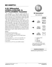
3.3V差分LVPECL / LVDS / CML到LVTTL / LVCMOS翻译 3.3V Differential LVPECL/LVDS/CML to LVTTL/LVCMOS Translator
Pictures:
3D模型
符号图
焊盘图
引脚图
产品图
页面导航:

导航目录
MC100EPT21MNR4数据手册
Page:
of 11 Go
若手册格式错乱,请下载阅览PDF原文件
MC100EPT21
http://onsemi.com
3
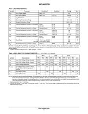
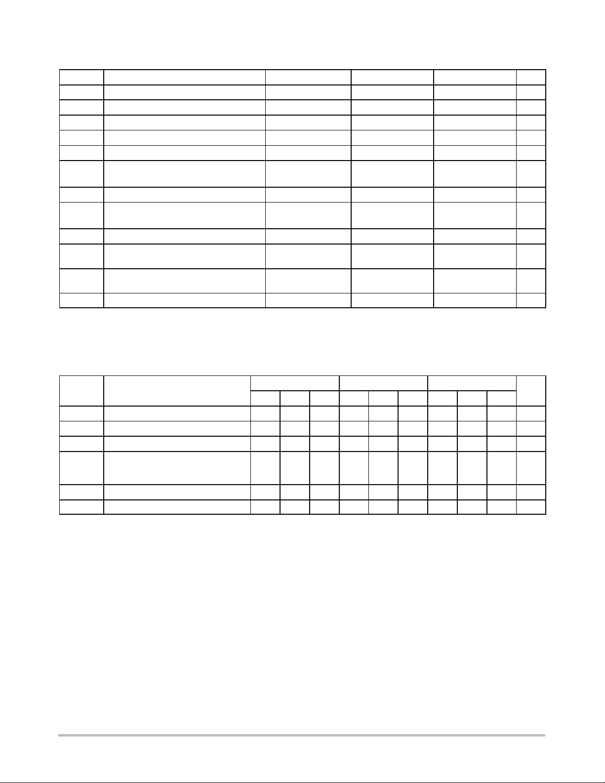
Table 3. MAXIMUM RATINGS
Symbol Parameter Condition 1 Condition 2 Rating Unit
V
CC
PECL Power Supply GND = 0 V 3.8 V
V
IN
PECL Input Voltage GND = 0 V V
I
V
CC
0 to 3.8 V
I
BB
V
BB
Sink/Source ± 0.5 mA
T
A
Operating Temperature Range −40 to +85 °C
T
stg
Storage Temperature Range −65 to +150 °C
q
JA
Thermal Resistance (Junction−to−Ambient) 0 lfpm
500 lfpm
SO−8
SO−8
190
130
°C/W
°C/W
q
JC
Thermal Resistance (Junction−to−Case) Standard Board SO−8 41 to 44 °C/W
q
JA
Thermal Resistance (Junction−to−Ambient) 0 lfpm
500 lfpm
TSSOP−8
TSSOP−8
185
140
°C/W
°C/W
q
JC
Thermal Resistance (Junction−to−Case) Standard Board TSSOP−8 41 to 44 °C/W
q
JA
Thermal Resistance (Junction−to−Ambient) 0 lfpm
500 lfpm
DFN8
DFN8
129
84
°C/W
°C/W
T
sol
Wave Solder Pb
Pb−Free
< 2 to 3 sec @ 248°C
<2 to 3 sec @ 260°C
265
265
°C
q
JC
Thermal Resistance (Junction−to−Case) (Note 2) DFN8 35 to 40 °C/W
Stresses exceeding Maximum Ratings may damage the device. Maximum Ratings are stress ratings only. Functional operation above the
Recommended Operating Conditions is not implied. Extended exposure to stresses above the Recommended Operating Conditions may affect
device reliability.
2. JEDEC standard multilayer board − 2S2P (2 signal, 2 power)
Table 4. PECL INPUT DC CHARACTERISTICS V
CC
= 3.3 V, GND = 0.0 V (Note 3)
Symbol Characteristic
−40°C 25°C 85°C
Unit
Min Typ Max Min Typ Max Min Typ Max
V
IH
Input HIGH Voltage (Single−Ended) 2075 2420 2075 2420 2075 2420 mV
V
IL
Input LOW Voltage (Single−Ended) 1355 1675 1355 1675 1355 1675 mV
V
BB
Output Voltage Reference 1775 1875 1975 1775 1875 1975 1775 1875 1975 mV
V
IHCMR
Input HIGH Voltage Common Mode
Range (Differential Configuration)
(Note 4)
1.2 3.3 1.2 3.3 1.2 3.3 V
I
IH
Input HIGH Current 150 150 150
mA
I
IL
Input LOW Current −150 −150 −150
mA
NOTE: Device will meet the specifications after thermal equilibrium has been established when mounted in a test socket or printed circuit
board with maintained transverse airflow greater than 500 lfpm. Electrical parameters are guaranteed only over the declared
operating temperature range. Functional operation of the device exceeding these conditions is not implied. Device specification limit
values are applied individually under normal operating conditions and not valid simultaneously.
3. Input parameters vary 1:1 with V
CC
.
4. V
IHCMR
min varies 1:1 with GND, V
IHCMR
max varies 1:1 with V
CC
. The V
IHCMR
range is referenced to the most positive side of the
differential input signal.
器件 Datasheet 文档搜索
AiEMA 数据库涵盖高达 72,405,303 个元件的数据手册,每天更新 5,000 多个 PDF 文件
