Datasheet 搜索 > 运算放大器 > Microchip(微芯) > MCP609T-I/ST 数据手册 > MCP609T-I/ST 其他数据使用手册 2/32 页
 器件3D模型
¥ 3.598
MCP609T-I/ST 其他数据使用手册 - Microchip(微芯)
制造商:
Microchip(微芯)
分类:
运算放大器
封装:
TSSOP-14
Pictures:
3D模型
符号图
焊盘图
引脚图
产品图
页面导航:
导航目录
MCP609T-I/ST数据手册
Page:
of 32 Go
若手册格式错乱,请下载阅览PDF原文件
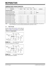
MCP606/7/8/9
DS11177E-page 2 © 2008 Microchip Technology Inc.
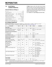
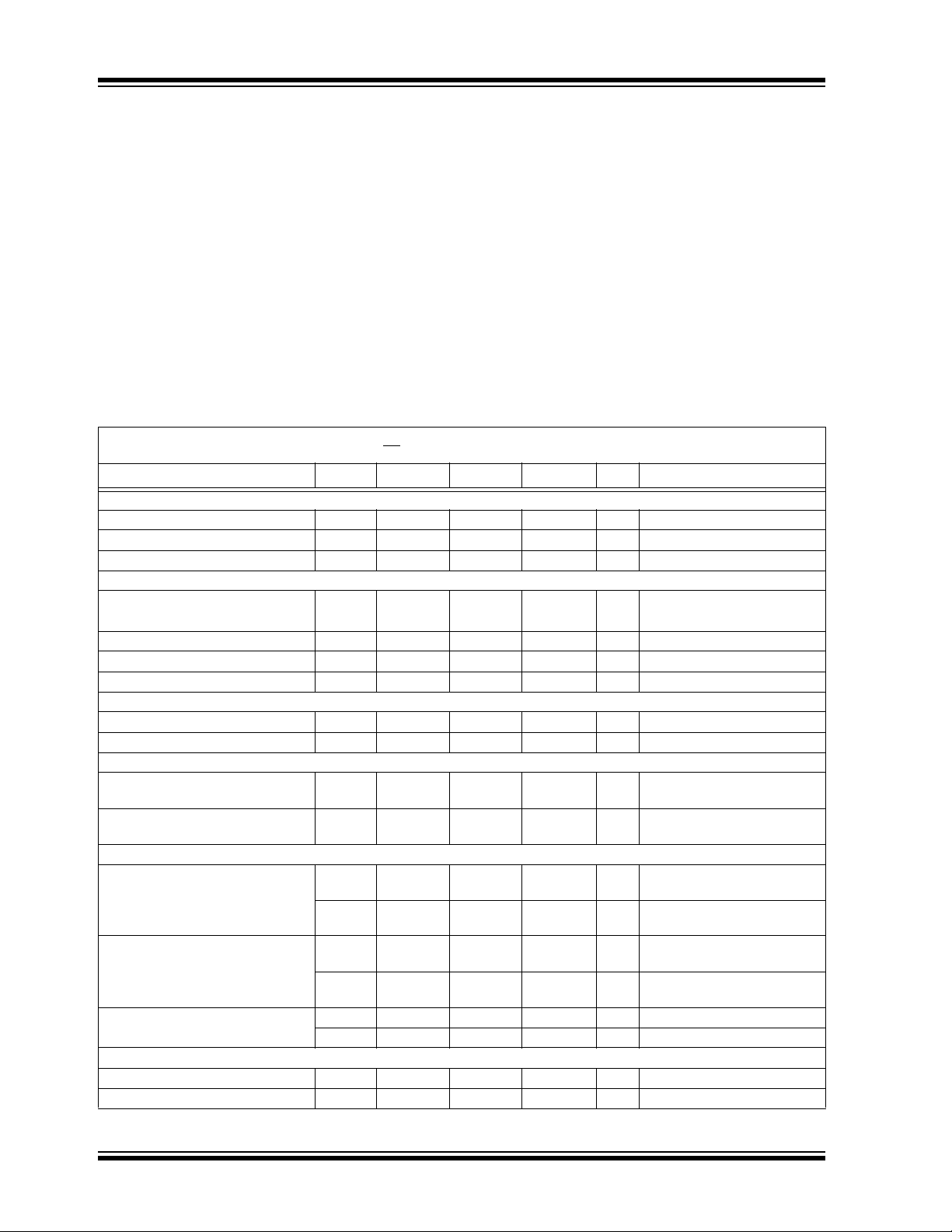
1.0 ELECTRICAL
CHARACTERISTICS
Absolute Maximum Ratings †
V
DD
–V
SS
........................................................................7.0V
Current at Input Pins ....................................................±2 mA
Analog Inputs (V
IN
+, V
IN
–) ††........ V
SS
–1.0VtoV
DD
+1.0V
All Other Inputs and Outputs ......... V
SS
– 0.3V to V
DD
+0.3V
Difference Input Voltage ...................................... |V
DD
–V
SS
|
Output Short Circuit Current .................................Continuous
Current at Output and Supply Pins ............................±30 mA
Storage Temperature..................................–65° C to +150° C
Maximum Junction Temperature (T
J
).........................+150° C
ESD Protection On All Pins (HBM; MM).............. ≥ 3 kV; 200V
† Notice: Stresses above those listed under “Absolute
Maximum Ratings” may cause permanent damage to the
device. This is a stress rating only and functional operation of
the device at those or any other conditions above those
indicated in the operational listings of this specification is not
implied. Exposure to maximum rating conditions for extended
periods may affect device reliability.
†† See Section 4.1.2 “Input Voltage and Current Limits”.
DC CHARACTERISTICS
Electrical Characteristics: Unless otherwise indicated, V
DD
= +2.5V to +5.5V, V
SS
=GND, T
A
=+25°C, V
CM
=V
DD
/2,
V
OUT
≈ V
DD
/2, V
L
= V
DD
/2, R
L
= 100 kΩ to V
L
, and CS is tied low (refer to Figure 1-2 and Figure 1-3).
Parameters Sym Min Typ Max Units Conditions
Input Offset
Input Offset Voltage V
OS
-250 — +250 µV
Input Offset Drift with Temperature ΔV
OS
/ΔT
A
—±1.8—µV/°CT
A
= -40°C to +85°C
Power Supply Rejection Ratio PSRR 80 93 — dB
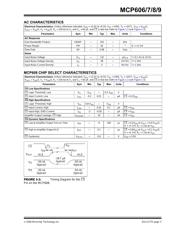
Input Bias Current and Impedance
Input Bias Current I
B
—1—pA
At Temperature I
B
——80pAT
A
= +85°C
Input Offset Bias Current I
OS
—1—pA
Common Mode Input Impedance Z
CM
—10
13
||6 — Ω||pF
Differential Input Impedance Z
DIFF
—10
13
||6 — Ω||pF
Common Mode
Common Mode Input Range V
CMR
V
SS
–0.3 V
DD
– 1.1 V CMRR ≥ 75 dB
Common Mode Rejection Ratio CMRR 75 91 — dB V
DD
= 5V, V
CM
= -0.3V to 3.9V
Open-Loop Gain
DC Open-Loop Gain
(Large-signal)
A
OL
105 121 — dB R
L
= 25 kΩ to V
L
,
V
OUT
= 50 mV to V
DD
–50mV
DC Open-Loop Gain
(Large-signal)
A
OL
100 118 — dB R
L
= 5 kΩ to V
L
,
V
OUT
= 0.1V to V
DD
–0.1V
Output
Maximum Output Voltage Swing V
OL
, V
OH
V
SS
+15 — V
DD
–20 mV R
L
= 25 kΩ to V
L
,
0.5V input overdrive
V
OL
, V
OH
V
SS
+45 — V
DD
–60 mV R
L
= 5 kΩ to V
L
,
0.5V input overdrive
Linear Output Voltage Range V
OUT
V
SS
+50 — V
DD
–50 mV R
L
= 25 kΩ to V
L
,
A
OL
≥ 105 dB
V
OUT
V
SS
+100 — V
DD
– 100 mV R
L
= 5 kΩ to V
L
,
A
OL
≥ 100 dB
Output Short Circuit Current I
SC
—7—mAV
DD
= 2.5V
I
SC
—17—mAV
DD
= 5.5V
Power Supply
Supply Voltage V
DD
2.5 — 6.0 V
Quiescent Current per Amplifier I
Q
— 18.7 25 µA I
O
= 0
Note 1: All parts with date codes November 2007 and later have been screened to ensure operation at V
DD
= 6.0V. However,
the other minimum and maximum specifications are measured at 2.5V and 5.5V.
器件 Datasheet 文档搜索
AiEMA 数据库涵盖高达 72,405,303 个元件的数据手册,每天更新 5,000 多个 PDF 文件
