Datasheet 搜索 > 光耦合器/光隔离器 > Fairchild(飞兆/仙童) > MCT5211SR2VM 数据手册 > MCT5211SR2VM 其他数据使用手册 2/13 页


¥ 0
MCT5211SR2VM 其他数据使用手册 - Fairchild(飞兆/仙童)
制造商:
Fairchild(飞兆/仙童)
分类:
光耦合器/光隔离器
Pictures:
3D模型
符号图
焊盘图
引脚图
产品图
页面导航:
导航目录
MCT5211SR2VM数据手册
Page:
of 13 Go
若手册格式错乱,请下载阅览PDF原文件
©1983 Fairchild Semiconductor Corporation www.fairchildsemi.com
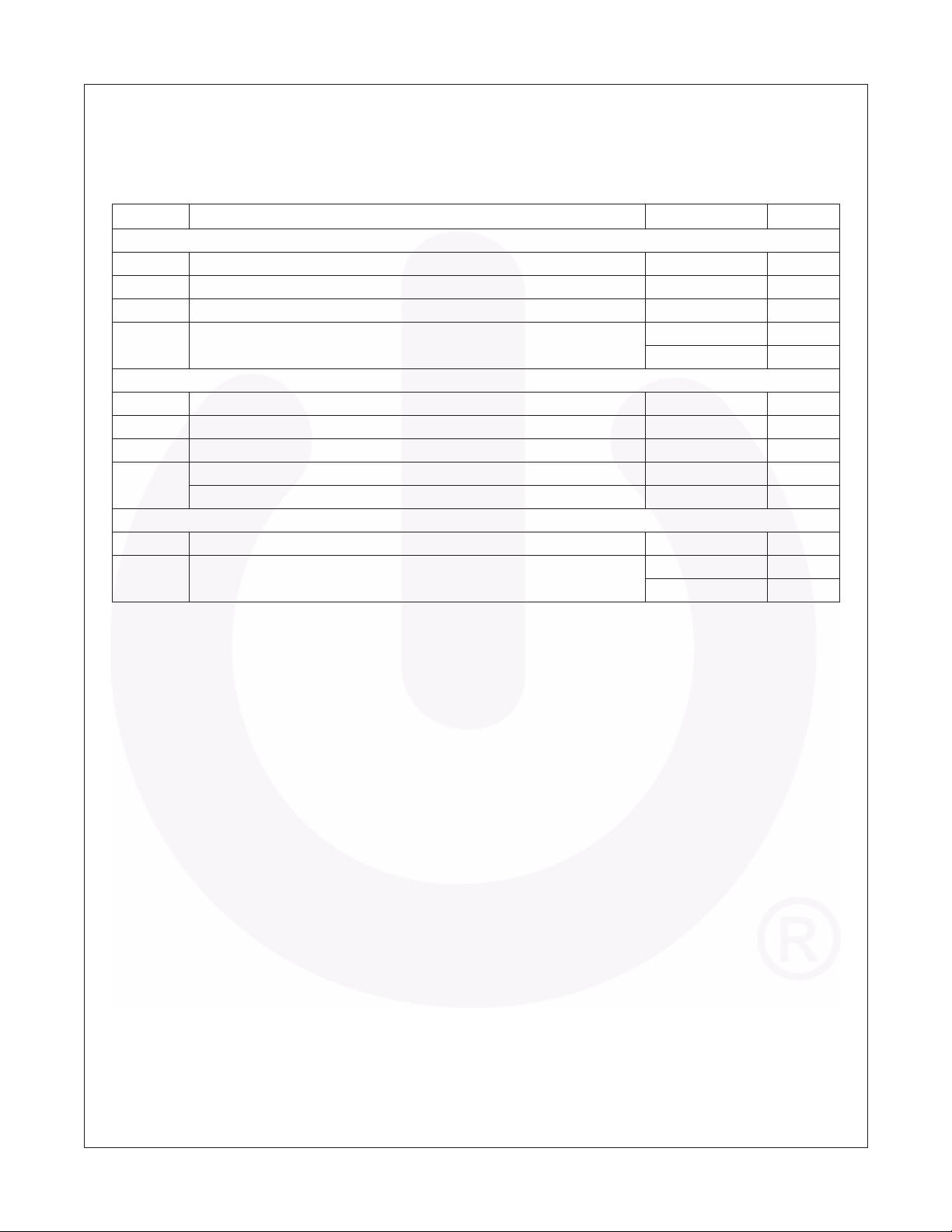
MCT5201M, MCT5210M, MCT5211M Rev. 1.1.3 2
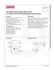
MCT5201M, MCT5210M, MCT5211M — Low Input Current Phototransistor Optocouplers
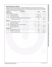
Absolute Maximum Ratings
Stresses exceeding the absolute maximum ratings may damage the device. The device may not function or be
operable above the recommended operating conditions and stressing the parts to these levels is not recommended.
In addition, extended exposure to stresses above the recommended operating conditions may affect device reliability.
The absolute maximum ratings are stress ratings only.
Symbol Parameters Value Units
TOTAL DEVICE
T
STG
Storage Temperature -55 to +150 °C
T
OPR
Operating Temperature -40 to +100 °C
T
SOL
Lead Solder Temperature 260 for 10 sec °C
P
D
Total Device Power Dissipation @ 25°C (LED plus detector) 260 mW
Derate Linearly From 25°C 3.5 mW/°C
EMITTER
I
F
Continuous Forward Current 50 mA
V
R
Reverse Input Voltage 6 V
I
F
(pk) Forward Current - Peak (1 µs pulse, 300 pps) 3.0 A
P
D
LED Power Dissipation 75 mW
Derate Linearly From 25°C 1.0 mW/°C
DETECTOR
I
C
Continuous Collector Current 150 mA
P
D
Detector Power Dissipation 150 mW
Derate Linearly from 25°C 2.0 mW/°C
器件 Datasheet 文档搜索
AiEMA 数据库涵盖高达 72,405,303 个元件的数据手册,每天更新 5,000 多个 PDF 文件
