Datasheet 搜索 > AC-DC转换器 > ON Semiconductor(安森美) > NCP1055P44G 数据手册 > NCP1055P44G 其他数据使用手册 2/27 页
 器件3D模型
¥ 4.309
NCP1055P44G 其他数据使用手册 - ON Semiconductor(安森美)
制造商:
ON Semiconductor(安森美)
分类:
AC-DC转换器
封装:
DIP-8
描述:
不需要辅助偏置绕组/欠压锁定/热关闭
Pictures:
3D模型
符号图
焊盘图
引脚图
产品图
页面导航:
典型应用电路图在P1P2
原理图在P3
封装尺寸在P24P26
型号编码规则在P1P22P23P27
标记信息在P1P25P26P27
封装信息在P22P23
功能描述在P2
应用领域在P1P16
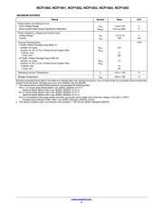
电气规格在P7P8P9
型号编号列表在P6
导航目录
NCP1055P44G数据手册
Page:
of 27 Go
若手册格式错乱,请下载阅览PDF原文件
NCP1050, NCP1051, NCP1052, NCP1053, NCP1054, NCP1055
www.onsemi.com
2
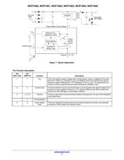
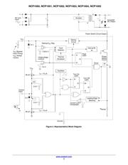
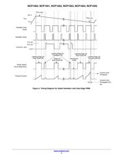
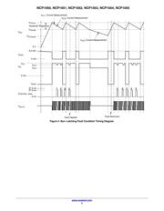
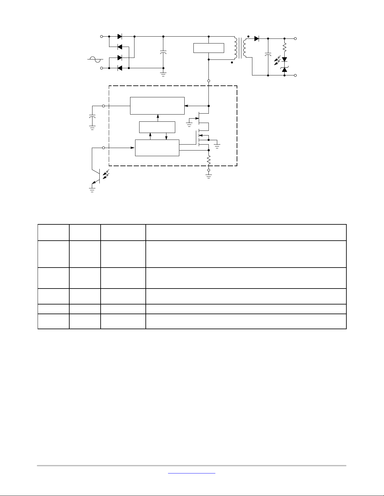
Figure 1. Typical Application
Startup & V
CC
Regulator Circuit
V
CC
Fault Detector
Power
Switch
Circuit
Oscillator &
Gating Logic
Control Input
Power Switch Circuit Output
3, 7−8
1
2
5
+
Snubber
+
+
+
−
Converter
DC Output
AC Line
Input
Ground
Pin Function Description
Pin
(SOT−223)
Pin
(PDIP−8)
Function Description
1 1 V
CC
This is the positive supply voltage input. During startup, power is supplied to this input
from Pin 5. When V
CC
reaches V
CC
(on), the Startup Circuit turns off and the output is
allowed to begin switching with 1.0 V hysteresis on the V
CC
pin. The capacitance con-
nected to this pin programs fault timing and frequency modulation rate.
2 2 Control Input
The Power Switch Circuit is turned off when a current greater than approximately 50 A
is drawn out of or applied to this pin. A 10 V clamp is built onto the chip to protect the
device from ESD damage or overvoltage conditions.
4 3, 7, 8 Ground This pin is the control circuit and Power Switch Circuit ground. It is part of the integrated
circuit lead frame.
− 4 No Connection
3 5 Power Switch
Drain
This pin is designed to directly drive the converter transformer primary, and internally
connects to Power Switch and Startup Circuit.
器件 Datasheet 文档搜索
AiEMA 数据库涵盖高达 72,405,303 个元件的数据手册,每天更新 5,000 多个 PDF 文件
