Datasheet 搜索 > ON Semiconductor(安森美) > NCP4305DDR2G 数据手册 > NCP4305DDR2G 其他数据使用手册 1/54 页
 器件3D模型
¥ 4.176
NCP4305DDR2G 其他数据使用手册 - ON Semiconductor(安森美)
制造商:
ON Semiconductor(安森美)
封装:
SOIC-8
描述:
SMPS拓扑
Pictures:
3D模型
符号图
焊盘图
引脚图
产品图
页面导航:
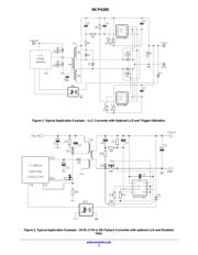
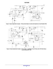
典型应用电路图在P1P2P3P35
原理图在P48
封装尺寸在P50P51P52
焊盘布局在P50P51P52
型号编码规则在P1P49P54
标记信息在P1P49P50P51P52P54
封装信息在P49
功能描述在P4P15
技术参数、封装参数在P5P49
应用领域在P1
电气规格在P6P7
型号编号列表在P5

导航目录
NCP4305DDR2G数据手册
Page:
of 54 Go
若手册格式错乱,请下载阅览PDF原文件
© Semiconductor Components Industries, LLC, 2016
June, 2016 − Rev. 3
1 Publication Order Number:
NCP4305/D
NCP4305
Secondary Side
Synchronous Rectification
Driver for High Efficiency
SMPS Topologies
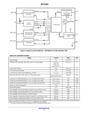
The NCP4305 is high performance driver tailored to control a
synchronous rectification MOSFET in switch mode power supplies.
Thanks to its high performance drivers and versatility, it can be used in
various topologies such as DCM or CCM flyback, quasi resonant
flyback, forward and half bridge resonant LLC.
The combination of externally adjustable minimum off-time and
on-time blanking periods helps to fight the ringing induced by the PCB
layout and other parasitic elements. A reliable and noise less operation
of the SR system is insured due to the Self Synchronization feature. The
NCP4305 also utilizes Kelvin connection of the driver to the MOSFET
to achieve high efficiency operation at full load and utilizes a light load
detection architecture to achieve high efficiency at light load.
The precise turn−off threshold, extremely low turn−off delay time
and high sink current capability of the driver allow the maximum
synchronous rectification MOSFET conduction time and enables
maximum SMPS efficiency. The high accuracy driver and 5 V gate
clamp enables the use of GaN FETs.
Features
• Self−Contained Control of Synchronous Rectifier in CCM, DCM and
QR for Flyback, Forward or LLC Applications
• Precise True Secondary Zero Current Detection
• Typically 12 ns Turn off Delay from Current Sense Input to Driver
• Rugged Current Sense Pin (up to 200 V)
• Ultrafast Turn−off Trigger Interface/Disable Input (7.5 ns)
• Adjustable Minimum ON−Time
• Adjustable Minimum OFF-Time with Ringing Detection
• Adjustable Maximum ON−Time for CCM Controlling of Primary
QR Controller
• Improved Robust Self Synchronization Capability
• 8 A / 4 A Peak Current Sink / Source Drive Capability
• Operating Voltage Range up to V
CC
= 35 V
• Automatic Light−load & Disable Mode
• Adaptive Gate Drive Clamp
• GaN Transistor Driving Capability (options A and C)
• Low Startup and Disable Current Consumption
• Maximum Operation Frequency up to 1 MHz
• SOIC-8 and DFN−8 (4x4) and WDFN8 (2x2) Packages
• These are Pb−Free Devices
Typical Applications
• Notebook Adapters
• High Power Density AC/DC Power Supplies (Cell
Phone Chargers)
• LCD TVs
• All SMPS with High Efficiency Requirements
SOIC−8
D SUFFIX
CASE 751
MARKING
DIAGRAMS
4305x = Specific Device Code
x = A, B, C, D or Q
A = Assembly Location
L = Wafer Lot
Y = Year
W = Work Week
M = Date Code
G = Pb−Free Package
1
8
NCP4305x
ALYW G
G
1
8
(Note: Microdot may be in either location)
4305x
ALYWG
G
1
DFN8
MN SUFFIX
CASE 488AF
www.onsemi.com
See detailed ordering and shipping information on page 49 o
f
this data sheet.
ORDERING INFORMATION
5xMG
G
1
WDFN8
MT SUFFIX
CASE 511AT
器件 Datasheet 文档搜索
AiEMA 数据库涵盖高达 72,405,303 个元件的数据手册,每天更新 5,000 多个 PDF 文件
