Datasheet 搜索 > RAM芯片 > Microchip(微芯) > PIC16F18854-I/SP 数据手册 > PIC16F18854-I/SP 其他数据使用手册 3/17 页
 器件3D模型
¥ 12.665
PIC16F18854-I/SP 其他数据使用手册 - Microchip(微芯)
制造商:
Microchip(微芯)
分类:
RAM芯片
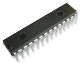
封装:
DIP-28
描述:
PIC 32MHz 闪存:4K@x14bit RAM:512Byte
Pictures:
3D模型
符号图
焊盘图
引脚图
产品图
页面导航:
原理图在P12
技术参数、封装参数在P14
电气规格在P14

导航目录
PIC16F18854-I/SP数据手册
Page:
of 17 Go
若手册格式错乱,请下载阅览PDF原文件
2016 Microchip Technology Inc. DS80000698B-page 3
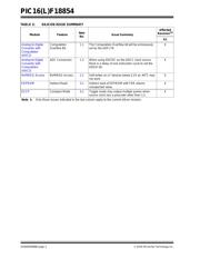
PIC16(L)F18854
Silicon Errata Issues
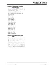
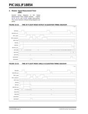
1. Module: Analog-to-Digital Converter with
Computation (ADC2)
1.1 Computation Overflow Bit
If the sign bit of ADFLTR (bit 7 of ADFLTRH) is set,
the Computation Overflow bit will also be set, even
though this is not a legitimate case of an overflow
event.
Work around
None.
Affected Silicon Revisions
1.2 ADC Conversion
When using ADCRC as the clock source for
ADCC, there is a delay of one instruction cycle
between the user setting the ADGO bit and being
able to read it set. This can lead to a false
conversion complete scenario (i.e., ADGO being
cleared), depending if the user code has a bit clear
test (BTFSC) instruction on the ADGO bit,
immediately after setting the ADGO bit. See code
example below.
e.g.
BSF ADCON0, ADGO ; Start conversion
BTFSC ADCON0, ADGO ; Is conversion done?
GOTO $-1 ; No, test again
The BTFSC will pass the very first time in this
situation
Work around
Add a NOP instruction after setting the ADGO bit
and before testing the bit for completion of
conversion. See code example below.
e.g.
BSF ADCON0, ADGO ; Start conversion
NOP
BTFSC ADCON0, ADGO ; Is conversion done?
GOTO $-1; No, test again
Affected Silicon Revisions
2. Module: Nonvolatile Memory Control
2.1 NVMREG Access
When performing self-writes through NVMREG
access on PIC16LF18854 devices with VDD below
2.2V and temperature of -40°C, the writes may not
work. This applies to both PFM and EEPROM
writes.
Work around
None.
Affected Silicon Revisions
3. Module: EEPROM
3.1 Indirect Read
Performing FSR reads of Data EEPROM
addresses other than the lowest address
(FSR=7000h) will return unexpected values.
Work around
Set NVMADRH:L to the desired address (F000h
through F0FFh) and retrieve the EEPROM value
from the NVMDATL register by setting the
NVMREGS and RD bits in the NVMCON1 register.
Affected Silicon Revisions
4. Module: ECCP
4.1 Compare Mode
The ECCP Compare Toggle modes
(CCPxCON<3:0> bits = 0010 or 0001) output
multiple pulses instead of a single toggle pulse
when its source clock has a prescaler other than
1:1.
Work around
Use CCP Compare mode with pulse output
(CCPxCON<3:0> bits = 1011) to clock a CLC
configured as a J-K flip-flop in Toggle mode.
Affected Silicon Revisions
Note: This document summarizes all silicon
errata issues from all revisions of silicon,
previous as well as current. Only the
issues indicated by the shaded column in
the following tables apply to the current
silicon revision (A1).
A1
X
A1
X
A1
X
A1
X
A1
X
器件 Datasheet 文档搜索
AiEMA 数据库涵盖高达 72,405,303 个元件的数据手册,每天更新 5,000 多个 PDF 文件
