Datasheet 搜索 > 微控制器 > Microchip(微芯) > PIC18F458-I/PT 数据手册 > PIC18F458-I/PT 其他数据使用手册 3/8 页
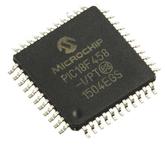
 器件3D模型
¥ 108.004
PIC18F458-I/PT 其他数据使用手册 - Microchip(微芯)
制造商:
Microchip(微芯)
分类:
微控制器
封装:
TQFP-44
描述:
MICROCHIP PIC18F458-I/PT 微控制器, 8位, 闪存, PIC18F, 40 MHz, 32 KB, 1.5 KB, 44 引脚, TQFP
Pictures:
3D模型
符号图
焊盘图
引脚图
产品图
PIC18F458-I/PT数据手册
Page:
of 8 Go
若手册格式错乱,请下载阅览PDF原文件

© 2006 Microchip Technology Inc. DS80161J-page 3
PIC18FXX8
7. Module: CAN
An incoming CAN message may not be saved
properly to a CAN receive buffer if one of the
following conditions is met:
1. Bank 15 is selected and the firmware attempts
to read the RXB0 or RXB1 registers while a
CAN message reception is in progress.
2. Bank 15 is selected and an instruction is
executed whose lower 8 bits match with one of
the CAN receive buffer addresses (RXBn
addresses in the range of 0xF61 to 0xF6E and
0xF51 to 0xF5D) while a CAN message recep-
tion is in progress. Some of the instruction
examples are:
• 0xFF68 (NOP)
• 0xEE68 (first half of GOTO 0xD0)
•0x0E6A (MOVLW 0x6A)
• 0x6055 (MOVF 0xF66, W)
Other instruction combinations exist.
3. The firmware attempts to access the GPR
(General Purpose Register) addresses
between addresses 0x51 and 0x5D in the
Access Bank while a CAN message reception is
in progress. Some of the instruction examples
are:
• MOVWF 0x57, A
• ADDWF 0x57, A
• MOVF 0x57, W, A
Work around
1. Once in normal CAN mode, never select
Bank 15. Always use Access Bank RAM to
access the CAN buffers. The RXB0 buffer is
already available in the Access Bank. All other
transmit and receive buffers are available in
Access Bank RAM, via the RXB0 registers,
using the WIN bits available in the CANCON
register.
2. Always make sure that the RXFUL bit is set
before attempting to access any of the Receive
Buffer registers.
3. Do not access/use any of the registers in the
Access Bank address range of 0x051 to
0x05D. If using assembly language, do not
allocate any of your application variables in this
address range. If using a C compiler, make
sure that the compiler does not allocate any
variable in the specified address range.
8. Module: Reset
It has been observed that in certain Reset condi-
tions, including power-up, the first GOTO instruction
at address 0x0000 may not be executed. This
occurrence is rare and affects very few applications.
To determine if your system is affected, test a
statistically significant number of applications across
the operating temperature, voltage and frequency
ranges of the application. Affected systems will
repeatedly fail normal testing. Systems not affected
will continue to not be affected over time.
Work around
Insert a NOP instruction at address 0x0000.
Date Codes that pertain to this issue:
All engineering and production devices.
器件 Datasheet 文档搜索
AiEMA 数据库涵盖高达 72,405,303 个元件的数据手册,每天更新 5,000 多个 PDF 文件
