Datasheet 搜索 > MOS管 > ST Microelectronics(意法半导体) > STD2N105K5 数据手册 > STD2N105K5 产品封装文件 5/21 页

¥ 6.99
STD2N105K5 产品封装文件 - ST Microelectronics(意法半导体)
制造商:
ST Microelectronics(意法半导体)
分类:
MOS管
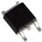
封装:
TO-252-3
描述:
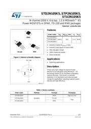
晶体管, MOSFET, N沟道, 1.5 A, 1.05 kV, 6 ohm, 10 V, 4 V
Pictures:
3D模型
符号图
焊盘图
引脚图
产品图
页面导航:
导航目录
STD2N105K5数据手册
Page:
of 21 Go
若手册格式错乱,请下载阅览PDF原文件
DocID026321 Rev 3 5/21
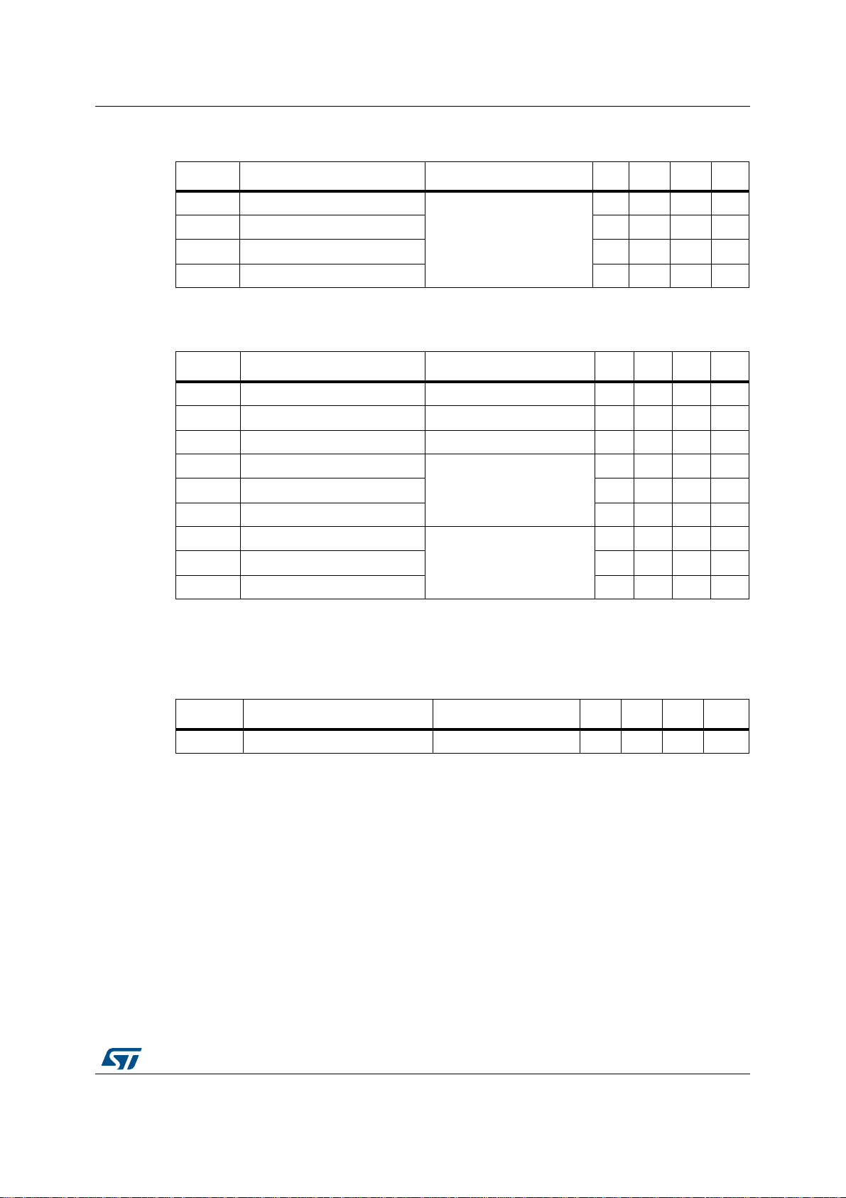
STD2N105K5, STP2N105K5, STU2N105K5 Electrical characteristics
21
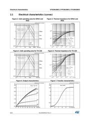
The built-in back-to-back Zener diodes have specifically been designed to enhance the
device's ESD capability. In this respect the Zener voltage is appropriate to achieve an
efficient and cost-effective intervention to protect the device's integrity. These integrated
Zener diodes thus avoid the usage of external components.
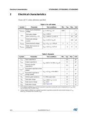
Table 6. Switching times
Symbol Parameter Test conditions Min. Typ. Max Unit
t
d(on)
Turn-on delay time
V
DD
= 525 V, I
D
= 0.75 A,
R
G
= 4.7 Ω, V
GS
= 10 V
(see Figure 17)
- 14.5 - ns
t
r
Rise time - 8.5 - ns
t
d(off)
Turn-off-delay time - 35 - ns
t
f
Fall time - 38.5 - ns
Table 7. Source drain diode
Symbol Parameter Test conditions Min. Typ. Max Unit
I
SD
Source-drain current - 1.5 A
I
SDM
(1)
1. Pulse width limited by safe operating area
Source-drain current (pulsed) - 6 A
V
SD
(2)
2. Pulsed: pulse duration = 300 µs, duty cycle 1.5%
Forward on voltage I
SD
= 1.5 A, V
GS
= 0 - 1.5 V
t
rr
Reverse recovery time
I
SD
= 1.5 A, di/dt = 100 A/µs
V
DD
= 60 V
(see Figure 19)
- 326 ns
Q
rr
Reverse recovery charge - 1.19 µC
I
RRM
Reverse recovery current - 7.3 A
t
rr
Reverse recovery time
I
SD
= 1.5 A, di/dt = 100 A/µs
V
DD
= 60 V T
J
= 150 °C
(see Figure 19)
- 525 ns
Q
rr
Reverse recovery charge - 1.83 µC
I
RRM
Reverse recovery current - 7 A
Table 8. Gate-source Zener diode
Symbol Parameter Test conditions Min Typ. Max. Unit
V
(BR)GSO
Gate-source breakdown voltage I
GS
= ± 1mA, I
D
=0 30 - - V
器件 Datasheet 文档搜索
AiEMA 数据库涵盖高达 72,405,303 个元件的数据手册,每天更新 5,000 多个 PDF 文件
