Datasheet 搜索 > MOS管 > ST Microelectronics(意法半导体) > STD7N52DK3 数据手册 > STD7N52DK3 产品封装文件 4/19 页

¥ 7.636
STD7N52DK3 产品封装文件 - ST Microelectronics(意法半导体)
制造商:
ST Microelectronics(意法半导体)
分类:
MOS管
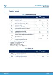
封装:
TO-252-3
描述:
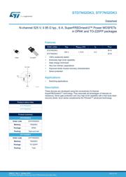
STMICROELECTRONICS STD7N52DK3 晶体管, MOSFET, N沟道, 6 A, 525 V, 0.95 ohm, 10 V, 3.75 V
Pictures:
3D模型
符号图
焊盘图
引脚图
产品图
页面导航:
导航目录
STD7N52DK3数据手册
Page:
of 19 Go
若手册格式错乱,请下载阅览PDF原文件
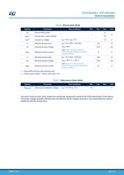
Table 6. Source-drain diode
Symbol Parameter Test conditions Min. Typ. Max. Unit
I
SD
Source-drain current
-
6
A
I
SDM
(1)
Source-drain current (pulsed) 24
V
SD
(2)
Forward on voltage
I
SD
= 6 A, V
GS
= 0 V
- 1.5 V
t
rr
Reverse recovery time
I
SD
= 6 A, di/dt = 100 A/µs,
V
DD
= 60 V
(see Figure 18. Test circuit for
inductive load switching and diode
recovery times)
-
110 ns
Q
rr
Reverse recovery charge 0.44 μC
I
RRM
Reverse recovery current 8 A
t
rr
Reverse recovery time
I
SD
= 6 A, di/dt = 100 A/µs,
V
DD
= 60 V, T
j
= 150 °C
(see Figure 18. Test circuit for
inductive load switching and diode
recovery times)
-
140 ns
Q
rr
Reverse recovery charge 0.68 μC
I
RRM
Reverse recovery current 10 A
1. Pulse width limited by safe operating area.
2. Pulsed: pulse duration = 300 µs, duty cycle 1.5%.
Table 7. Gate-source Zener diode
Symbol
Parameter Test conditions Min. Typ. Max. Unit
V
(BR)GSO
Gate-source breakdown voltage
I
GS
= ±1 mA, I
D
= 0 A
30 - - V
The built-in back-to-back Zener diodes are specifically designed to enhance the ESD performance of the device.
The Zener voltage facilitates efficient and cost-effective device integrity protection, thus eliminating the need for
additional external componentry.
STD7N52DK3, STF7N52DK3
Electrical characteristics
DS6515 - Rev 3
page 4/19
器件 Datasheet 文档搜索
AiEMA 数据库涵盖高达 72,405,303 个元件的数据手册,每天更新 5,000 多个 PDF 文件
