Datasheet 搜索 > 开发套件 > TI(德州仪器) > ADC08D1520DEV/NOPB 数据手册 > ADC08D1520DEV/NOPB 产品设计参考手册 3/18 页


¥ 18422.588
ADC08D1520DEV/NOPB 产品设计参考手册 - TI(德州仪器)
制造商:
TI(德州仪器)
分类:
开发套件
Pictures:
3D模型
符号图
焊盘图
引脚图
产品图
页面导航:
导航目录
ADC08D1520DEV/NOPB数据手册
Page:
of 18 Go
若手册格式错乱,请下载阅览PDF原文件

3
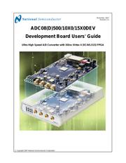
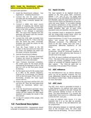
1.0 Introduction
The ADC08(D)XXXXDEV Board is designed to allow
quick evaluation and design development of National
Semiconductor’s ADC08(D)XXXX ultra high speed 8-bit
Analog-to-Digital Converters. Reference to
ADC08(D)XXXX through out this document applies to the
following devices: ADC08500, ADC08D500, ADC081000,
ADC08D1000, ADC08D1020, ADC081500,
ADC08D1500, and ADC08D1520.
The ADC08500, ADC081000 and ADC081500 have a
single channel input with a sampling rate of 500 MSPS,
1.0 GSPS and 1.5 GSPS, respectively. The ADC08D500,
ADC08D10X0 and ADC08D15X0 are specified for 500
MSPS, 1.0 GSPS, and 1.5 GSPS operation in 2-input
channel mode, respectively. The ADC08D10X0, and
ADC08D15X0 may be configured to sample at 2 GSPS or
3 GSPS, respectively, in Dual Edge Sampling (DES)
mode.
This development board is designed to function with
National Semiconductor’s WaveVision Software, for fast
evaluation. It requires only three connections to get
started: a power supply, a USB Interface to a PC, and a
signal source. An on-board clock generator is provided,
and the system also allows for an external clock to be
used if alternate sample rates are required.
The ADC connects to a Xilinx Virtex4 FPGA which stores
up to 4K of data from each channel before transferring it
through the USB interface to the PC.
2.0 Board Assembly
The ADC08(D)XXXXDEV Development Board comes in a
low profile plastic enclosure and does not require assisted
cooling due to its low power consumption. The
ADC08(D)XXXX device is configured entirely through
software and also allows changes to easily be made to
the FPGA configuration to enable system development.
3.0 Board Specifications
The following shows the board specifications for the
ADC08(D)XXXX, Table 1.
Board Size: 168 mm x 100 mm
Power
Requirements:
+12V, 800 mA
Clock Frequency
Range (25° C) :
ADC08(D)500DEV: 150 MHz - 700 MHz
ADC08(D)10X0DEV: 500 MHz - 1.0 GHz
ADC08(D)15X0DEV: 800 MHz - 1.5 GHz
Analog Input Range
(AC Coupled):
30 MHz to 1800 MHz
Nominal Analog
Input Voltage:
560 mV
P-P
to 870 mV
P-P
Analog Input
Impedance:
50 Ohms
Table 1. Board Specifications
3.1 FPGA Specification
The board supports a Xilinx LX15 Virtex 4 363-pin FPGA.
This device is responsible for collecting and storing the
data from ADC, measuring the clock frequency, and
uploading the data through the microcontroller to the PC.
Three separate FPGA images are used to support clock
speeds at 500 MHz, 1 GHz, and 1.5 GHz. The 500 MHz
image typically supports a clock range of 150 MHz to 700
MHz. The 1 GHz image typically supports a clock range
of 500 MHz to 1.0 GHz, while the 1.5 GHz image typically
supports a clock range of 800 MHz to 1.5 GHz.
Normally, the FPGA is configured automatically by the
WaveVision software. It is possible, through modification
of the board, to configure the FPGA using a FLASH ROM,
so that the system may be run without the USB
microcontroller.
NOTE: Though the development board provides a
powerful capability for the user to develop his own
FPGA code, National does not support such custom
FPGA code development.
3.2 Microcontroller
A Cypress CY7C68013A microcontroller manages the
USB interface and general control of the board hardware
(for Evaluation boards REV 2.0 and above). It uses a 24
MHz crystal oscillator.
3.3 Memory Components
One 2K EEPROM (24C02 or similar) is connected to the
I
2
C Bus for Microcontroller and USB configuration data.
This EEPROM also identifies the ADC and clock source.
3.4 Power Supplies
Power to the board is supplied through a single-pin power
jack to allow the use of an external brick power supply
with a voltage range of 8V to 12V.
器件 Datasheet 文档搜索
AiEMA 数据库涵盖高达 72,405,303 个元件的数据手册,每天更新 5,000 多个 PDF 文件
