Datasheet 搜索 > 开发套件 > TI(德州仪器) > ADC08D1520DEV/NOPB 数据手册 > ADC08D1520DEV/NOPB 产品设计参考手册 5/18 页


¥ 18422.588
ADC08D1520DEV/NOPB 产品设计参考手册 - TI(德州仪器)
制造商:
TI(德州仪器)
分类:
开发套件
Pictures:
3D模型
符号图
焊盘图
引脚图
产品图
页面导航:
导航目录
ADC08D1520DEV/NOPB数据手册
Page:
of 18 Go
若手册格式错乱,请下载阅览PDF原文件
5
3.8 ADC Analog Inputs
The analog inputs (I- and Q-channel) are provided
through SMA connectors on the front edge of the board
and are single-ended. The ADC I-channel input is
capable of accepting an AC- or DC-coupled input signal.
The Q-channel may be AC-coupled only.
Single-ended to differential input signal conversion is
performed by a Mini-Circuits Balun (ADTL2-18) for the
AC-coupled path. A LMH6555 Differential Op-Amp is
used to DC couple the input signal. Software-controlled
Teledyne RF relays are used to switch the signal path
from AC- to DC-coupled.
3.9 Trigger Input
A trigger input is provided on the front panel through a
SMA connector. This signal is connected to the FPGA
via a Schmitt trigger and is TTL compatible with 5V
tolerance. This input has no functionality, and is
provided so the user may develop his own FPGA
functionality if desired.
3.10 Status Indicators
The Following Status Indicators (LEDs) are provided on
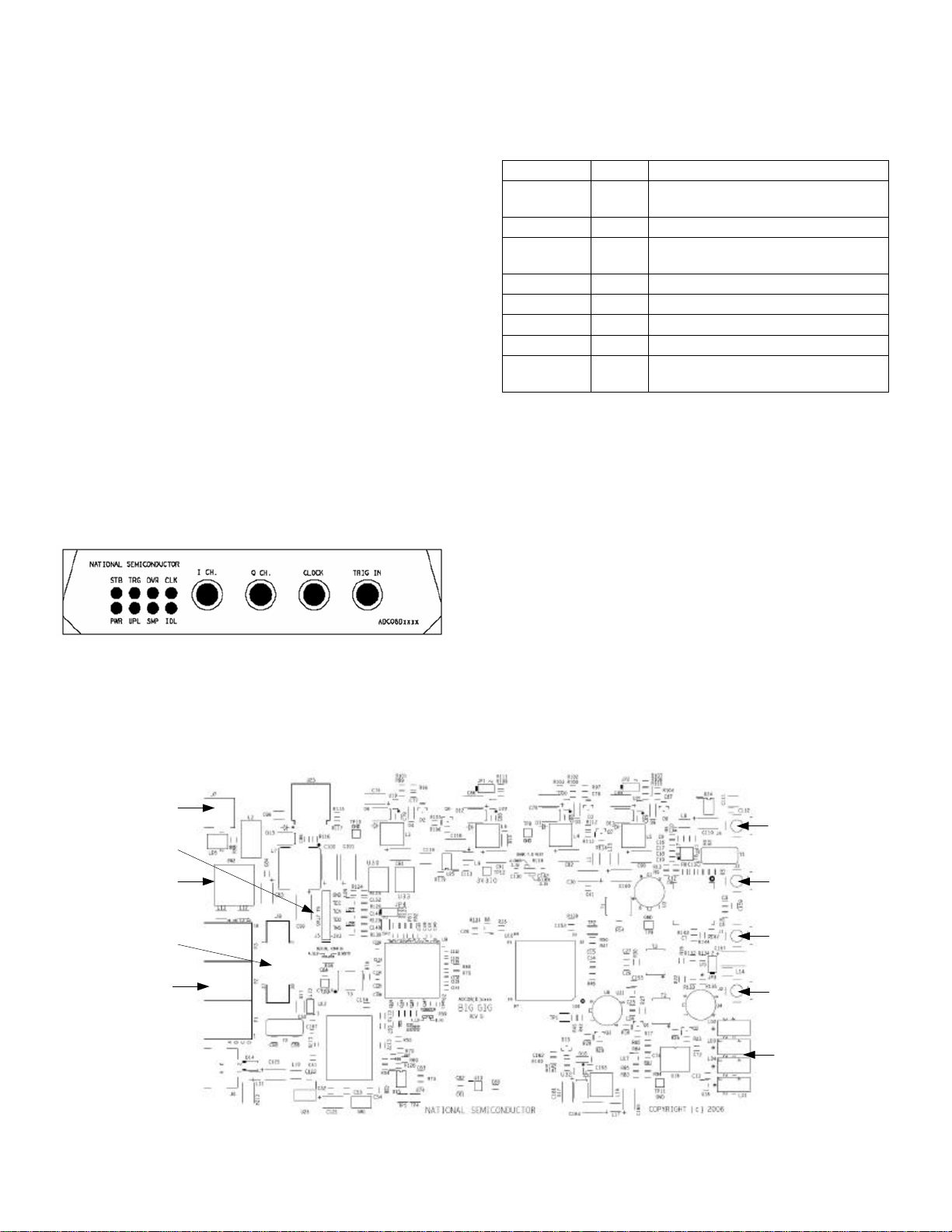
the front edge of the board, Figure2:
Figure 2. Component placement and front panel
This is a brief summary of the name, abbreviation and
description of the status LEDs:
Name Abbr. Description
Standby STB
All switching regulators powered
down
Trigger TRG Trigger input indicator
Over-
range OVR Over-range indicator
Clock CLK Clock active indicator (blinks)
Power-on PWR 12V-30V power
Upload UPL Data is being uploaded to PC
Sample SMP Data is being captured by FPGA
FPGA
RDY/IDLE IDL FPGA is programmed and IDLE
Table 2. Status Indicators
3.11 Debug
A Mictor Logic Analyzer Header is provided along with
test-point headers both of which are connected to the
FPGA. This allows monitoring of captured data and
critical signals during board debug. A JTAG header is
also provided to allow further FPGA development.
_________________________________________________________________________________________________________________________
4.0 Quick Start
Refer to Figure 3 for the location of the power
connection, signal input and USB port.
PWR
Input
JTAG
Header
PWR
Switch
MICTOR
Header
Expansion
Header
Trigger
Input
Clock
Input
Analog
Q-CH. Input
Analog
I-CH. Input
Status
LEDS
Figure 3. Development board overview
器件 Datasheet 文档搜索
AiEMA 数据库涵盖高达 72,405,303 个元件的数据手册,每天更新 5,000 多个 PDF 文件
