Datasheet 搜索 > 开发套件 > TI(德州仪器) > ADC08D1520DEV/NOPB 数据手册 > ADC08D1520DEV/NOPB 产品设计参考手册 6/18 页


¥ 18429.251
ADC08D1520DEV/NOPB 产品设计参考手册 - TI(德州仪器)
制造商:
TI(德州仪器)
分类:
开发套件
Pictures:
3D模型
符号图
焊盘图
引脚图
产品图
页面导航:
导航目录
ADC08D1520DEV/NOPB数据手册
Page:
of 18 Go
若手册格式错乱,请下载阅览PDF原文件

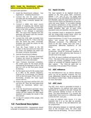
NOTE: Install the WaveVision4 software
before connecting this product to the PC.
For quick start operation:
1. Install the WaveVision4 software. See
Appendix B – Installing WaveVision.
2. Connect the 12V DC power source
(included with the development board) to
the rear Power Connector labeled (8V-
12V DC).
3. Connect a stable sine wave source
capable of supplying the desired input
frequencies at up to 8 dBm. Connect this
signal to the front panel SMA connector
labeled “I CH.” through a band-pass
filter. The exact level required from the
generator will depend upon the insertion
loss of the filter used.
4. Connect the USB cable (included) from
the USB port to the PC. If this is the first
time the board has been connected,
Windows may install the drivers for this
product at this time.
5. Push the Power Switch to the ON
position on the rear panel and check that
the Green LED between the switch and
the power connector illuminates.
6. Start the WaveVision4 Software.
7. Once loaded, the “Firmware Download”
Progress bar should be displayed. See
Appendix B for more information.
8. Upon Firmware Download completion,
the control panel for the board should
automatically be displayed on the PC and
the CLK LED on the front panel should
be flashing.
9. Set the signal source for the analog input
to 8 dBm at the desired frequency.
Observe the Out-of-Range LED labeled
OVR on the front panel. If this LED is not
illuminated, increase the input signal
source until it is.
10. Reduce the input level until the OVR LED
just turns off. Now, the input signal level
should be maximized, without over-
ranging.
11. From the WaveVision4 pull-down menu
select Acquire and then Samples. The
system will then capture the input signal
waveform and display the results in the
time domain.
12. For the FFT analysis of this sample, click
the FFT Tab.
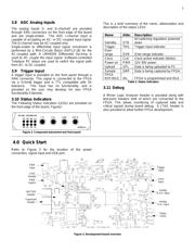
5.0 Functional Description
The ADC08(D)XXXXDEV Development Board
schematic is included as an additional document.
5.1 Input circuitry
The input signal(s) to be digitized should be
applied to the front panel SMA connectors
labeled “I CH.” and “Q CH.” For single input
devices such as the ADC08500, ADC081000 and
ADC0815000, apply the signal only to the “I CH.”
These 50 Ohm inputs are intended to accept low-
noise sine wave signals. To accurately evaluate
the dynamic performance of this converter, the
analog input signal(s) must be filtered by a high-
quality bandpass filter with at least 10-bit
equivalent noise and distortion characteristics.
This evaluation board is designed for operation
with two single-ended analog inputs, which are
converted to differential signals on-board.
Signal transformers T2 and T3 are connected as
baluns, and provide the single-ended to
differential conversion. The differential PCB
traces to the ADC analog input pins have a
characteristic differential impedance of 100
Ohms.
No other test equipment, such as an
oscilloscope, should be connected anywhere in
the signal path while gathering data because it
will add noise to the signal.
The TRIG_IN input is buffered and passed to the
FPGA. The intent of this input is to allow users to
expand the existing capabilities of the current
system by providing for external triggering of a
data capture. The TRIG_IN input has no
functionality in the provided FPGA firmware.
5.2 ADC reference
The ADC08(D)XXXX has an internal reference
which can not be adjusted. However, the Full-
Scale (differential) Range may be adjusted with
the Software Control Panel. Refer to Section 6.0
for more information
5.3 ADC clock
The ADC clock, which is generated on-board, is
a fixed frequency. An external clock signal may
alternatively be supplied to the ADC through the
SMA Connector labeled “CLOCK” on the front
panel. The balun-transformer (T1) converts the
single-ended clock source to a differential signal
to drive the ADC clock pins.
If using an external clock source, it is very
important that it is as low jitter as possible.
Otherwise, the SNR of the ADC08(D)XXXX will
be compromised.
When alternating between an externally applied
clock to the on-board clock, the clock input
should never be left floating. The user is advised
器件 Datasheet 文档搜索
AiEMA 数据库涵盖高达 72,405,303 个元件的数据手册,每天更新 5,000 多个 PDF 文件
