Datasheet 搜索 > ON Semiconductor(安森美) > FDG6321C 数据手册 > FDG6321C 产品设计参考手册 4/9 页


¥ 1.221
FDG6321C 产品设计参考手册 - ON Semiconductor(安森美)
制造商:
ON Semiconductor(安森美)
封装:
SOT-363-6
描述:
双路场效应管, MOSFET, 互补N与P沟道, 25 V, 500 mA, 0.45 ohm, SC-70, 表面安装
Pictures:
3D模型
符号图
焊盘图
引脚图
产品图
页面导航:
型号编码规则在P9
标记信息在P1P9
技术参数、封装参数在P8
应用领域在P7

导航目录
FDG6321C数据手册
Page:
of 9 Go
若手册格式错乱,请下载阅览PDF原文件
Rev. A, March 2004
3
©2004 Fairchild Semiconductor Corporation
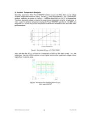
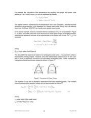
4. Junction Temperature Analysis
Generally, breakdown of the Power MOSFET seldom occurs even if the drain-source voltage
exceeds the absolute maximum rating. The BV
DSS
of the Power MOSFET has a positive tem-
perature coefficient as shown in Figure 4. It reaches about 990V at 120°C in this example.
Therefore, a greater voltage is required to cause device breakdown at higher temperature. In
many cases, the ambient temperature during the Power MOSFET operation is over 25°C and
the power loss causes the junction temperature of the Power MOSFET to rise above the ambi-
ent temperature.
Figure 4. Normalized BV
DSS
vs Tj, FQA11N90C
Also, note that the BV
DSS
in Figure 4 is measured at 250µA of the drain current. In a real
breakdown, the drain current reaches a much higher level and the breakdown voltage is even
higher than the above value.
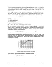
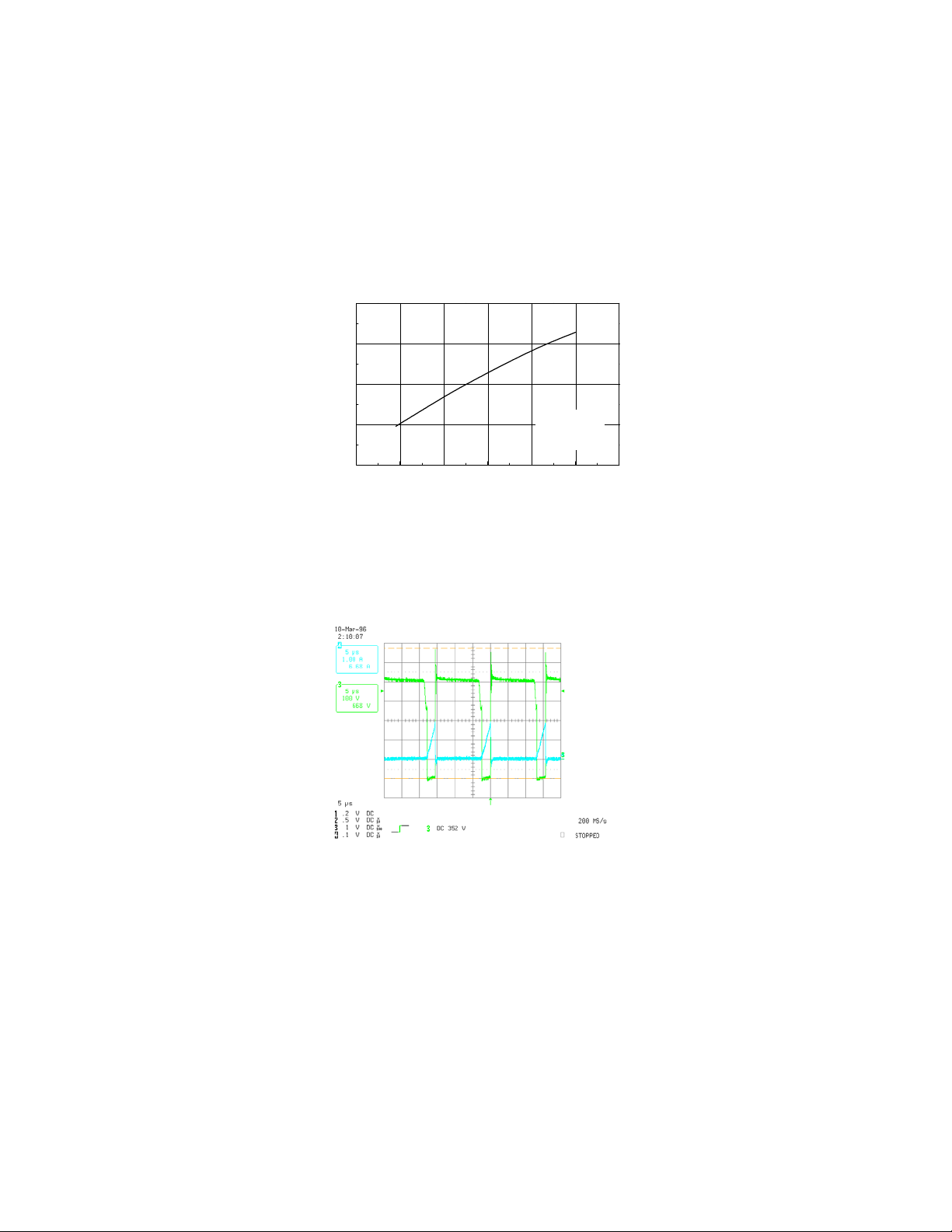
Figure 5. Waveforms from Switching Power Supply,
600V rated MOSFET
-100 -50 0 50 100 150 200
0.8
0.9
1.0
1.1
1.2
Notes :※
1. V
GS
= 0 V
2. I
D
= 250 µ A
BV
DSS
, (Normalized)
Drain-Source Breakdown Voltage
T
J
, Junction Temperature [
o
C]
器件 Datasheet 文档搜索
AiEMA 数据库涵盖高达 72,405,303 个元件的数据手册,每天更新 5,000 多个 PDF 文件
