Datasheet 搜索 > NXP(恩智浦) > MCIMX287CVM4C 数据手册 > MCIMX287CVM4C 产品设计参考手册 5/20 页
 器件3D模型
¥ 32.314
MCIMX287CVM4C 产品设计参考手册 - NXP(恩智浦)
制造商:
NXP(恩智浦)
封装:
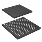
MAPBGA-289
Pictures:
3D模型
符号图
焊盘图
引脚图
产品图
MCIMX287CVM4C数据手册
Page:
of 20 Go
若手册格式错乱,请下载阅览PDF原文件
i.MX28 Layout and Design Guidelines, Rev. 0
Freescale Semiconductor 5
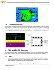
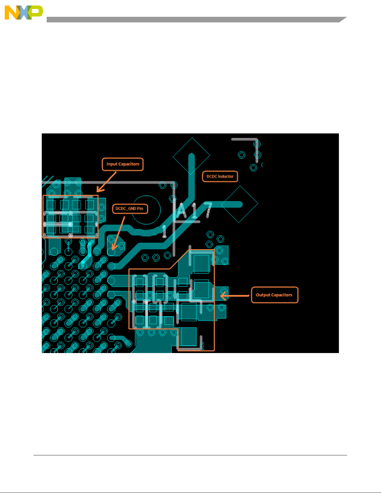
PMU and DC-DC Converter
• Place the DCDC output capacitors as close as possible to their respective DCDC output pins (less
than 5mm away): DCDC_VDDIO, DCDC_VDDA, DCDC_VDDD.
• Place the ground connections of the DCDC_BATT input capacitors as close as possible to both the
DCDC_GND pin and the ground connections of the DCDC output capacitors.
• Place the ground connections of the DCDC output capacitors as close as possible to both the
DCDC_GND pin and the ground connections of the DCDC_BATT pin input capacitors.
The drawing below shows an optimal layout for the top layer placement and routing of the DCDC
converter.
3.3 Battery Connection
• Route the positive battery terminal on the power plane layer using a minimum trace width of 30
mils (0.762mm). A thicker trace may be required for longer battery trace runs (using a plane is
best).
• Connect the negative battery terminal directly to the ground plane(s) as well as to the top and
bottom ground fill using multiple vias (3 or more).
器件 Datasheet 文档搜索
AiEMA 数据库涵盖高达 72,405,303 个元件的数据手册,每天更新 5,000 多个 PDF 文件
