Datasheet 搜索 > 微控制器 > TI(德州仪器) > MSP430FR5739CY 数据手册 > MSP430FR5739CY 产品设计参考手册 4/578 页

¥ 5.999
MSP430FR5739CY 产品设计参考手册 - TI(德州仪器)
制造商:
TI(德州仪器)
分类:
微控制器
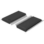
封装:
DIE
描述:
其他系列 24MHz 16K@x8bitFRAM 1KB
Pictures:
3D模型
符号图
焊盘图
引脚图
产品图
页面导航:
引脚图在P24Hot
原理图在P62P72P89P244P266P329P336P358P383P411P428P435
应用领域在P39P41P73P578
导航目录
MSP430FR5739CY数据手册
Page:
of 578 Go
若手册格式错乱,请下载阅览PDF原文件

www.ti.com
4.4.3 Symbolic Mode .................................................................................................. 103
4.4.4 Absolute Mode .................................................................................................. 108
4.4.5 Indirect Register Mode ......................................................................................... 110
4.4.6 Indirect Autoincrement Mode .................................................................................. 111
4.4.7 Immediate Mode ................................................................................................ 112
4.5 MSP430 and MSP430X Instructions .................................................................................. 114
4.5.1 MSP430 Instructions ............................................................................................ 114
4.5.2 MSP430X Extended Instructions .............................................................................. 119
4.6 Instruction Set Description .............................................................................................. 130
4.6.1 Extended Instruction Binary Descriptions .................................................................... 131
4.6.2 MSP430 Instructions ............................................................................................ 133
4.6.3 Extended Instructions .......................................................................................... 185
4.6.4 Address Instructions ............................................................................................ 228
5 FRAM Controller (FRCTL) ................................................................................................. 243
5.1 FRAM Introduction ....................................................................................................... 244
5.2 FRAM Organization ...................................................................................................... 244
5.3 FRCTL Module Operation .............................................................................................. 244
5.4 Programming FRAM Memory Devices ................................................................................ 245
5.4.1 Programming FRAM Memory by JTAG or Spy-Bi-Wire .................................................... 245
5.4.2 Programming FRAM Memory by Bootstrap Loader (BSL) ................................................ 245
5.4.3 Programming FRAM Memory by Custom Solution ......................................................... 245
5.5 Wait State Control ....................................................................................................... 245
5.5.1 Manual Wait State Control ..................................................................................... 245
5.5.2 Automatic Wait State Control .................................................................................. 246
5.5.3 Wait State and Cache Hit ...................................................................................... 246
5.5.4 Safe Access ..................................................................................................... 246
5.6 FRAM ECC ............................................................................................................... 246
5.7 FRCTL Registers ......................................................................................................... 247
5.7.1 FRCTL0 Register ............................................................................................... 248
5.7.2 GCCTL0 Register ............................................................................................... 249
5.7.3 GCCTL1 Register ............................................................................................... 250
6 Memory Protection Unit (MPU) .......................................................................................... 251
6.1 Memory Protection Unit (MPU) Introduction .......................................................................... 252
6.2 MPU Segments ........................................................................................................... 253
6.2.1 Main Memory Segments ....................................................................................... 253
6.2.2 Segment Border Setting ........................................................................................ 253
6.2.3 Information Memory ............................................................................................ 255
6.3 MPU Access Management Settings ................................................................................... 255
6.4 MPU Violations ........................................................................................................... 256
6.4.1 Interrupt Table and Reset Vector ............................................................................. 256
6.4.2 Violation Handling ............................................................................................... 256
6.5 MPU Registers ........................................................................................................... 257
6.5.1 MPUCTL0 Register ............................................................................................. 258
6.5.2 MPUCTL1 Register ............................................................................................. 259
6.5.3 MPUSEG Register .............................................................................................. 260
6.5.4 MPUSAM Register .............................................................................................. 261
6.5.5 MPUIV Register ................................................................................................. 263
7 DMA Controller ................................................................................................................ 264
7.1 Direct Memory Access (DMA) Introduction ........................................................................... 265
7.2 DMA Operation ........................................................................................................... 267
7.2.1 DMA Addressing Modes ....................................................................................... 267
7.2.2 DMA Transfer Modes ........................................................................................... 268
4
Contents SLAU272C–May 2011–Revised November 2013
Submit Documentation Feedback
Copyright © 2011–2013, Texas Instruments Incorporated
器件 Datasheet 文档搜索
AiEMA 数据库涵盖高达 72,405,303 个元件的数据手册,每天更新 5,000 多个 PDF 文件
