Datasheet 搜索 > 微控制器 > TI(德州仪器) > MSP430FR5739CY 数据手册 > MSP430FR5739CY 产品设计参考手册 5/578 页

¥ 5.996
MSP430FR5739CY 产品设计参考手册 - TI(德州仪器)
制造商:
TI(德州仪器)
分类:
微控制器
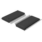
封装:
DIE
描述:
其他系列 24MHz 16K@x8bitFRAM 1KB
Pictures:
3D模型
符号图
焊盘图
引脚图
产品图
页面导航:
引脚图在P24Hot
原理图在P62P72P89P244P266P329P336P358P383P411P428P435
应用领域在P39P41P73P578
导航目录
MSP430FR5739CY数据手册
Page:
of 578 Go
若手册格式错乱,请下载阅览PDF原文件

www.ti.com
7.2.3 Initiating DMA Transfers ....................................................................................... 274
7.2.4 Halting Executing Instructions for DMA Transfers .......................................................... 275
7.2.5 Stopping DMA Transfers ....................................................................................... 275
7.2.6 DMA Channel Priorities ........................................................................................ 275
7.2.7 DMA Transfer Cycle Time ..................................................................................... 276
7.2.8 Using DMA With System Interrupts ........................................................................... 276
7.2.9 DMA Controller Interrupts ...................................................................................... 276
7.2.10 Using the eUSCI_B I
2
C Module With the DMA Controller ................................................ 277
7.2.11 Using ADC10 With the DMA Controller ..................................................................... 278
7.3 DMA Registers ........................................................................................................... 279
7.3.1 DMACTL0 Register ............................................................................................. 281
7.3.2 DMACTL1 Register ............................................................................................. 282
7.3.3 DMACTL2 Register ............................................................................................. 283
7.3.4 DMACTL3 Register ............................................................................................. 284
7.3.5 DMACTL4 Register ............................................................................................. 285
7.3.6 DMAxCTL Register ............................................................................................. 286
7.3.7 DMAxSA Register ............................................................................................... 288
7.3.8 DMAxDA Register ............................................................................................... 289
7.3.9 DMAxSZ Register ............................................................................................... 290
7.3.10 DMAIV Register ................................................................................................ 291
8 Digital I/O ........................................................................................................................ 292
8.1 Digital I/O Introduction ................................................................................................... 293
8.2 Digital I/O Operation ..................................................................................................... 294
8.2.1 Input Registers (PxIN) .......................................................................................... 294
8.2.2 Output Registers (PxOUT) ..................................................................................... 294
8.2.3 Direction Registers (PxDIR) ................................................................................... 294
8.2.4 Pullup or Pulldown Resistor Enable Registers (PxREN) .................................................. 294
8.2.5 Function Select Registers (PxSEL0, PxSEL1) .............................................................. 295
8.2.6 Port Interrupts ................................................................................................... 295
8.3 I/O Configuration ......................................................................................................... 297
8.3.1 Configuration After Reset ...................................................................................... 297
8.3.2 Configuration of Unused Port Pins ........................................................................... 297
8.3.3 Configuration for LPMx.5 Low-Power Modes ............................................................... 298
8.4 Digital I/O Registers ..................................................................................................... 300
8.4.1 P1IV Register .................................................................................................... 313
8.4.2 P2IV Register .................................................................................................... 313
8.4.3 P3IV Register .................................................................................................... 314
8.4.4 P4IV Register .................................................................................................... 314
8.4.5 PxIN Register .................................................................................................... 315
8.4.6 PxOUT Register ................................................................................................. 315
8.4.7 PxDIR Register .................................................................................................. 315
8.4.8 PxREN Register ................................................................................................. 316
8.4.9 PxSEL0 Register ................................................................................................ 316
8.4.10 PxSEL1 Register ............................................................................................... 316
8.4.11 PxSELC Register .............................................................................................. 317
8.4.12 PxIES Register ................................................................................................. 317
8.4.13 PxIE Register ................................................................................................... 317
8.4.14 PxIFG Register ................................................................................................. 318
9 CRC Module .................................................................................................................... 319
9.1 Cyclic Redundancy Check (CRC) Module Introduction ............................................................. 320
9.2 CRC Standard and Bit Order ........................................................................................... 320
9.3 CRC Checksum Generation ............................................................................................ 321
9.3.1 CRC Implementation ........................................................................................... 321
5
SLAU272C–May 2011–Revised November 2013 Contents
Submit Documentation Feedback
Copyright © 2011–2013, Texas Instruments Incorporated
器件 Datasheet 文档搜索
AiEMA 数据库涵盖高达 72,405,303 个元件的数据手册,每天更新 5,000 多个 PDF 文件
