Datasheet 搜索 > 微处理器 > NXP(恩智浦) > P1013NXN2HFB 数据手册 > P1013NXN2HFB 产品设计参考手册 4/84 页

¥ 1203.595
P1013NXN2HFB 产品设计参考手册 - NXP(恩智浦)
制造商:
NXP(恩智浦)
分类:
微处理器
封装:
BGA-689
描述:
PowerPC系列 1.055GHz
Pictures:
3D模型
符号图
焊盘图
引脚图
产品图
页面导航:
原理图在P11
导航目录
P1013NXN2HFB数据手册
Page:
of 84 Go
若手册格式错乱,请下载阅览PDF原文件

e500 Software Optimization Guide (eSOG), Rev. 0
4 Freescale Semiconductor
Preliminary—Subject to Change Without Notice
Overview
cannot execute in the proper clock cycle because data or resources needed to process the instruction
are not yet available.
• Superscalar—A superscalar processor is one that can issue multiple instructions concurrently from
a conventional linear instruction stream. In a superscalar implementation, multiple instructions can
execute in parallel at the same time.
• Throughput—The number of instructions that are processed per cycle. In particular, throughput
describes the performance of a multiple-stage pipeline where a sequence of instructions may pass
through with a throughput that is much faster than the latency of an individual instruction. For
example, in the four-stage multiple-cycle pipeline (MU), a series of mulli instructions has a
throughput of one instruction per clock cycle even though it takes 4 cycles for one mulli instruction
to execute.
• Write back—Write back (in the context of instruction handling) occurs when a result is written into
the architecture-defined registers (typically the GPRs). On the e500, write back occurs in the clock
cycle after the completion stage. Results in the write back buffer cannot be flushed. If an exception
occurs, results from previous instructions must write back before the exception is taken.
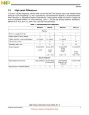
1.2 Processor Overview
This section gives an overview of the e500 core. Section 1.3, “High-Level Differences,” lists high-level
differences between the e500 core and other processors in the PowerPC family: MPC603e, a G2 processor
used in the 82xx family of integrated host and communication processors; a G3 MPC755; and an
MPC745x from the G4 family. Section 1.4, “Pipeline Differences,” describes the different pipelines of
these processors.
The MPC603e, MPC755, and MPC745x implement the 32-bit portion of the PowerPC architecture, which
provides 32-bit effective addresses, integer data types of 8, 16, and 32 bits and single- and double-precision
floating-point data types. In addition, the MPC745x implements the AltiVec
™
instruction set architectural
extension.
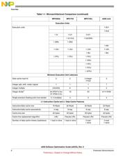
The e500 core implements the 32-bit portion of the Book E architecture, a PowerPC architecture definition
for embedded processors. Book E ensures binary compatibility with the user instruction set architecture
(UISA) portion of the PowerPC architecture. All classic PowerPC integer instructions (for example,
arithmetic, logical, load/store, and branch) are supported on e500 except lswi, lswx, stswi, and stswx.
Book E allows processors to provide auxiliary processing units (APUs), which are extensions to the
architecture that can perform computational or system management functions. The most significant of
these on the e500 is the signal processing engine (SPE) APU, which includes a suite of vector instructions
that use the upper and lower halves of the 64-bit general-purpose registers (GPRs) as a single two-element
operand (that is, an SIMD instructions). The SPE defines instructions that support vectors of fractional,
integer, and single-precision floating-point data types. In addition, the e500 core implements a scalar
single-precision floating-point APU..
Section 2, “e500 Core Processor,” provides an overview of the e500 core complex. Section 3, “e500 Core
Microarchitecture,” gives a detailed description of the e500 core microarchitecture.
器件 Datasheet 文档搜索
AiEMA 数据库涵盖高达 72,405,303 个元件的数据手册,每天更新 5,000 多个 PDF 文件
