Datasheet 搜索 > DSP数字信号处理器 > TI(德州仪器) > TMS320C6421ZDUQ5 数据手册 > TMS320C6421ZDUQ5 产品设计参考手册 2/222 页
 器件3D模型
¥ 45.62
TMS320C6421ZDUQ5 产品设计参考手册 - TI(德州仪器)
制造商:
TI(德州仪器)
分类:
DSP数字信号处理器
封装:
BGA-376
描述:
数字信号处理器和控制器 - DSP, DSC Fixed-Pt Dig Signal Proc
Pictures:
3D模型
符号图
焊盘图
引脚图
产品图
页面导航:
引脚图在P16P29P33P74P75P77P79P84P85P86P90P91Hot
原理图在P4P107P108P117P118P166P184
封装尺寸在P218
标记信息在P218P219
封装信息在P217P218P219
技术参数、封装参数在P109P113P114P115P116P117P118P119P120P121P122P123
应用领域在P2P110
电气规格在P106P111P112P113P114P115P116P117P118P119P120P121
导航目录
TMS320C6421ZDUQ5数据手册
Page:
of 222 Go
若手册格式错乱,请下载阅览PDF原文件

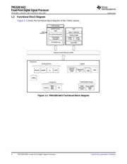
1.2 Description
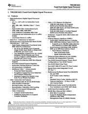
TMS320C6421
Fixed-Point Digital Signal Processor
SPRS346D – JANUARY 2007 – REVISED JUNE 2008
www.ti.com
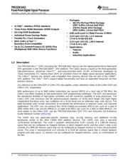
• Packages:
– 361-Pin Pb-Free PBGA Package
(ZWT Suffix), 0.8-mm Ball Pitch
• VLYNQ™ Interface (FPGA Interface)
– 376-Pin Plastic BGA Package
• Three Pulse Width Modulator (PWM) Outputs
(ZDU Suffix), 1.0-mm Ball Pitch
• On-Chip ROM Bootloader
• 0.09- µ m/6-Level Cu Metal Process (CMOS)
• Individual Power-Savings Modes
• 3.3-V and 1.8-V I/O, 1.2-V Internal
• Flexible PLL Clock Generators
(-7/-6/-5/-4/-Q6/-Q5/-Q4)
• IEEE-1149.1 (JTAG™)
• 3.3-V and 1.8-V I/O, 1.05-V Internal
Boundary-Scan-Compatible
(-7/-6/-5/-4/-L/-Q5)
• Up to 111 General-Purpose I/O (GPIO) Pins
• Applications:
(Multiplexed With Other Device Functions)
– Telecom
– Audio
– Industrial Applications
The TMS320C64x+™ DSPs (including the TMS320C6421 device) are the highest-performance fixed-point
DSP generation in the TMS320C6000™ DSP platform. The C6421 device is based on the third-generation
high-performance, advanced VelociTI™ very-long-instruction-word (VLIW) architecture developed by
Texas Instruments (TI), making these DSPs an excellent choice for digital signal processor applications.
The C64x+™ devices are upward code-compatible from previous devices that are part of the C6000™
DSP platform. The C64x™ DSPs support added functionality and have an expanded instruction set from
previous devices.
Any reference to the C64x DSP or C64x CPU also applies, unless otherwise noted, to the C64x+ DSP and
C64x+ CPU, respectively.
With performance of up to 5600 million instructions per second (MIPS) at a clock rate of 700 MHz, the
C64x+ core offers solutions to high-performance DSP programming challenges. The DSP core possesses
the operational flexibility of high-speed controllers and the numerical capability of array processors. The
C64x+ DSP core processor has 64 general-purpose registers of 32-bit word length and eight highly
independent functional units—two multipliers for a 32-bit result and six arithmetic logic units (ALUs). The
eight functional units include instructions to accelerate the performance in telecom, audio, and industrial
applications. The DSP core can produce four 16-bit multiply-accumulates (MACs) per cycle for a total of
2800 million MACs per second (MMACS), or eight 8-bit MACs per cycle for a total of 5600 MMACS. For
more details on the C64x+ DSP, see the TMS320C64x/C64x+ DSP CPU and Instruction Set Reference
Guide (literature number SPRU732 ).
The C6421 also has application-specific hardware logic, on-chip memory, and additional on-chip
peripherals similar to the other C6000 DSP platform devices. The C6421 core uses a two-level
cache-based architecture. The Level 1 program memory/cache (L1P) consists of a 128K-bit memory
space that can be configured as mapped memory or direct mapped cache, and the Level 1 data (L1D)
consists of a 384K-bit memory space that can be configured as mapped memory or 2-way set-associative
cache. The Level 2 memory/cache (L2) consists of a 512K-bit memory space that is shared between
program and data space. L2 memory can be configured as mapped memory, cache, or combinations of
the two.
2 TMS320C6421 Fixed-Point Digital Signal Processor Submit Documentation Feedback
器件 Datasheet 文档搜索
AiEMA 数据库涵盖高达 72,405,303 个元件的数据手册,每天更新 5,000 多个 PDF 文件
