Datasheet 搜索 > DSP数字信号处理器 > TI(德州仪器) > TMS320C6745DPTPD4 数据手册 > TMS320C6745DPTPD4 产品设计参考手册 4/218 页
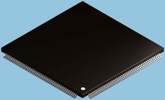
 器件3D模型
¥ 128.94
TMS320C6745DPTPD4 产品设计参考手册 - TI(德州仪器)
制造商:
TI(德州仪器)
分类:
DSP数字信号处理器
封装:
LQFP-176
描述:
DSP),Texas Instruments德州仪器数字信号处理器是微处理器,带有一个优化的体系结构,用于数字信号处理的运算需求。### 数字信号处理器,Texas Instruments
Pictures:
3D模型
符号图
焊盘图
引脚图
产品图
页面导航:
原理图在P18P157P162P163
应用领域在P16P218

导航目录
TMS320C6745DPTPD4数据手册
Page:
of 218 Go
若手册格式错乱,请下载阅览PDF原文件

www.ti.com
3.1 Introduction ................................................................................................................. 50
3.1.1 Purpose of the Level 1 Data (L1D) Memory and Cache .................................................... 50
3.1.2 Features ........................................................................................................... 50
3.1.3 Terms and Definitions ............................................................................................ 50
3.2 L1D Memory Architecture ................................................................................................ 50
3.2.1 L1D Memory ...................................................................................................... 50
3.3 L1D Cache ................................................................................................................. 51
3.3.1 L1D Cache Architecture ......................................................................................... 51
3.3.2 Replacement and Allocation Strategy ......................................................................... 52
3.3.3 L1D Mode Change Operations ................................................................................. 53
3.3.4 L1D Freeze Mode ................................................................................................ 54
3.3.5 Program-Initiated Cache Coherence Operations ............................................................. 56
3.3.6 Cache Coherence Protocol ..................................................................................... 58
3.4 L1D Cache Control Registers ............................................................................................ 59
3.4.1 Memory Mapped L1D Cache Control Register Overview ................................................... 59
3.4.2 CPU L1D Cache Control Registers ............................................................................ 59
3.4.3 L1D Cache Configuration Registers ........................................................................... 60
3.4.4 L1D Cache Coherence Operation Registers .................................................................. 62
3.4.5 Privilege and Cache Control Operations ...................................................................... 66
3.5 L1D Memory Performance ............................................................................................... 66
3.5.1 L1D Memory Banking ............................................................................................ 66
3.5.2 L1D Miss Penalty ................................................................................................. 68
3.5.3 L1D Write Buffer .................................................................................................. 68
3.5.4 L1D Miss Pipelining .............................................................................................. 69
3.6 L1D Power-Down Support ................................................................................................ 69
3.7 L1D Memory Protection ................................................................................................... 70
3.7.1 Protection Checks on L1D Accesses .......................................................................... 70
3.7.2 L1D Memory Protection Registers ............................................................................. 70
3.7.3 Protection Checks on Accesses to Memory Protection Registers ......................................... 79
4 Level 2 Memory and Cache ................................................................................................. 81
4.1 Introduction ................................................................................................................. 82
4.1.1 Purpose of the Level 2 (L2) Memory and Cache ............................................................. 82
4.1.2 Features ........................................................................................................... 82
4.1.3 Terms and Definitions ............................................................................................ 82
4.2 Level 2 Memory Architecture ............................................................................................ 82
4.2.1 L2 Memory ........................................................................................................ 82
4.3 L2 Cache ................................................................................................................... 84
4.3.1 L2 Cache Architecture ........................................................................................... 84
4.3.2 Replacement and Allocation Strategy ......................................................................... 85
4.3.3 Reset Behavior ................................................................................................... 85
4.3.4 L2 Mode Change Operations ................................................................................... 86
4.3.5 L2 Freeze Mode .................................................................................................. 87
4.3.6 Program Initiated Cache Coherence Operations ............................................................. 88
4.3.7 Cacheability Controls ............................................................................................ 90
4.3.8 L1-L2 Coherence Support ....................................................................................... 91
4.4 L2 Cache Control Registers .............................................................................................. 93
4.4.1 Memory Mapped L2 Cache Control Registers Overview ................................................... 93
4.4.2 L2 Configuration Register (L2CFG) ............................................................................ 94
4.4.3 L2 Cache Coherence Operation Registers ................................................................... 95
4.4.4 Memory Attribute Registers (MARn) .......................................................................... 100
4.4.5 Memory Attribute Registers (MARn) .......................................................................... 106
4.4.6 Privilege and Cache Control Registers ...................................................................... 106
4.5 L2 Power-Down .......................................................................................................... 107
4
Contents SPRUFK5A–August 2010
Copyright © 2010, Texas Instruments Incorporated
器件 Datasheet 文档搜索
AiEMA 数据库涵盖高达 72,405,303 个元件的数据手册,每天更新 5,000 多个 PDF 文件
