Datasheet 搜索 > 稳压芯片 > TI(德州仪器) > TPS7A8101QDRBRQ1 数据手册 > TPS7A8101QDRBRQ1 产品设计参考手册 3/9 页
 器件3D模型
¥ 5.767
TPS7A8101QDRBRQ1 产品设计参考手册 - TI(德州仪器)
制造商:
TI(德州仪器)
分类:
稳压芯片
封装:
VDFN-8
描述:
TPS7A8101QDRBRQ1 编带
Pictures:
3D模型
符号图
焊盘图
引脚图
产品图
页面导航:
原理图在P7
焊盘布局在P4
应用领域在P9
型号编号列表在P5

导航目录
TPS7A8101QDRBRQ1数据手册
Page:
of 9 Go
若手册格式错乱,请下载阅览PDF原文件
Vin
EN
Vout
Iout
www.ti.com
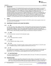
Operation
• Connect a 0-A to 100-mA load between an OUT pin at connector J4, and a GND pin at connector J3.
• Disable the output by connecting the jumper on JP1 from the EN pin to the OFF pin.
3 Operation
• Turn on the input power supply. For initial operation, set the input power supply, VIN – J1, to 10 V
• Enable the output by reconnecting the jumper on JP1 from the EN pin to the ON pin.
• Vary the respective loads and VIN voltages as necessary for test purposes.
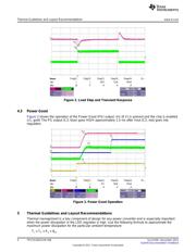
4 Test Results
This section provides typical performance waveforms for the TPS7A1601EVM-046 printed-circuit board.
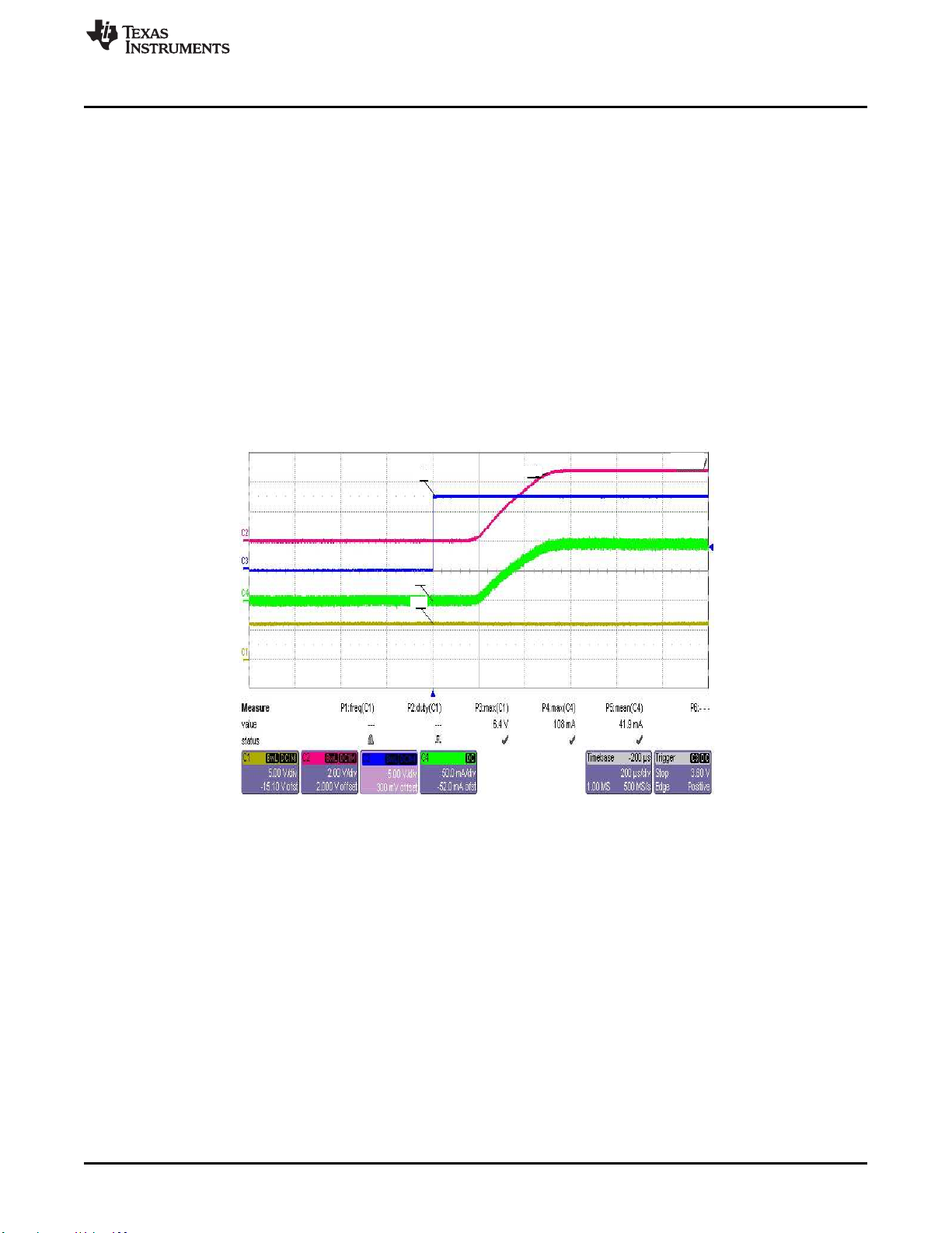
4.1 Turnon Sequence
Figure 1 shows the turnon/off characteristic where VIN is preset to 10 V, the output drives full load, and
the EN turnon is stepped to 10 V (C2, red). The output soft start (C1, yellow) shows a monotonic rise time
of approximately 60 ms. The output voltage start-up ramp is not load dependant.
Figure 1. Turnon Sequence
4.2 Output Load Transient
Figure 2 shows the load transient response (OUT – C1, yellow) for a full-load step transient from 10 mA to
100 mA (C4, green). VIN is set at 10 V.
3
SLVU549– December 2011 TPS7A1601EVM-046
Submit Documentation Feedback
Copyright © 2011, Texas Instruments Incorporated
器件 Datasheet 文档搜索
AiEMA 数据库涵盖高达 72,405,303 个元件的数据手册,每天更新 5,000 多个 PDF 文件
