Datasheet 搜索 > 稳压芯片 > TI(德州仪器) > TPS7A8101QDRBRQ1 数据手册 > TPS7A8101QDRBRQ1 产品设计参考手册 5/9 页
 器件3D模型
¥ 5.767
TPS7A8101QDRBRQ1 产品设计参考手册 - TI(德州仪器)
制造商:
TI(德州仪器)
分类:
稳压芯片
封装:
VDFN-8
描述:
TPS7A8101QDRBRQ1 编带
Pictures:
3D模型
符号图
焊盘图
引脚图
产品图
页面导航:
原理图在P7
焊盘布局在P4
应用领域在P9
型号编号列表在P5

导航目录
TPS7A8101QDRBRQ1数据手册
Page:
of 9 Go
若手册格式错乱,请下载阅览PDF原文件
www.ti.com
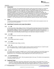
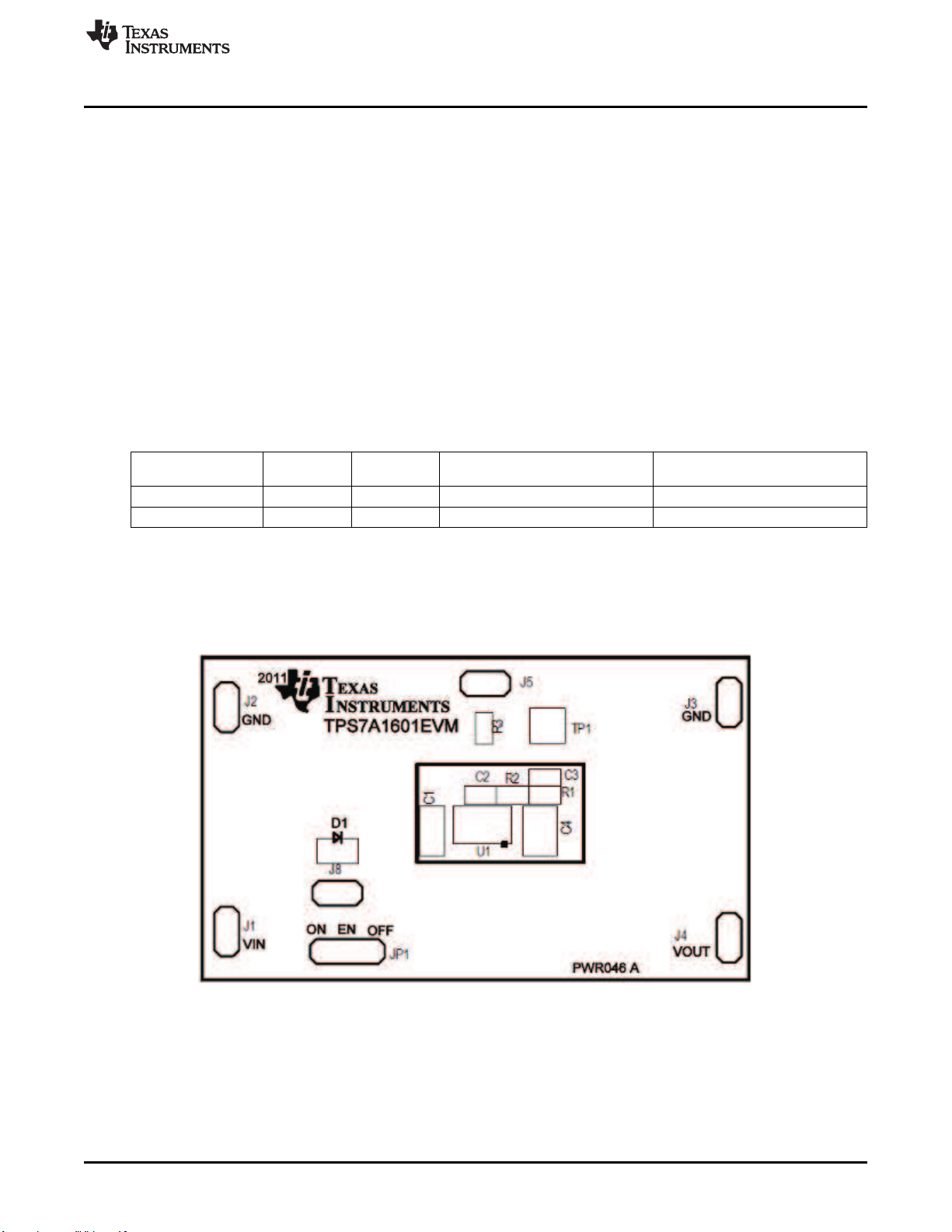
Board Layout
Where T
J
is the junction temperature, T
A
is the ambient temperature, P
D
is the power dissipation in the
device (W), and θ
JA
is the thermal resistance from junction to ambient. All temperatures are in degrees
Celsius. The maximum silicon junction temperature, T
J
, must not be allowed to exceed 150°C. The layout
design must use copper trace and plane areas effectively, as thermal sinks, in order not to allow T
J
to
exceed the absolute maximum rating under all temperature conditions and voltage conditions across the
part.
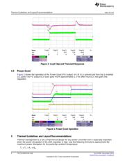
The designer must consider carefully the thermal design of the PCB for optimal performance over
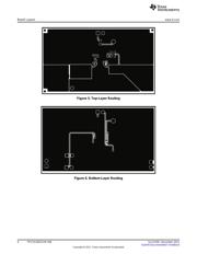
temperature. For this EVM, Figure 5 shows that the PCB top GND plane has six, 6-mil, thermal via
connections to the bottom-side copper GND plane to dissipate heat. The PCB is a two-layer board with
2-oz. copper on top and bottom layers. The DGN package drawing can be found at the Texas Instruments
Web site in the product folder for the TPS7A16xx LDO linear regulator.
Table 1 repeats information from the Dissipation Ratings Table of the TPS7A16xx data sheet for
comparison with the thermal resistance, θ
JA
, calculated for this EVM layout to show the wide variation in
thermal resistances for given copper areas. The High-K value is determined using a standard JEDEC
High-K (2s2p) board having dimensions of 3-inch x 3-inch with 1-oz internal power and ground planes and
2-oz copper traces on top and bottom of the board.
Table 1. Thermal Resistance, θ
JA
, and Maximum Power Dissipation
Max Dissipation without Derating Max Dissipation without Derating
Board Package θ
JA
(T
A
= 25°C) (T
A
= 70°C)
High-K DGN 55.09°C/W 1.8 mW 998 mW
TPS7A1601EVM-046 DGN 38.89°C/W 2.57 W 1.41.W
The thermal resistance for the TPS7A1601EVM-046, θ
JA
, is the measured value for this particular layout
scheme. The maximum power dissipation is proportional to the volume of copper volume connected to the
package.
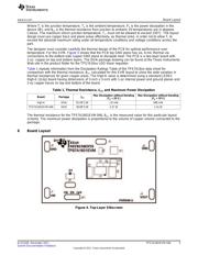
6 Board Layout
Figure 4. Top-Layer Silkscreen
5
SLVU549– December 2011 TPS7A1601EVM-046
Submit Documentation Feedback
Copyright © 2011, Texas Instruments Incorporated
器件 Datasheet 文档搜索
AiEMA 数据库涵盖高达 72,405,303 个元件的数据手册,每天更新 5,000 多个 PDF 文件
